
Sustainability
Peeking into a microscope in science class for the first time can be an unforgettable experience, and many people still recall the tingle of excitement. Electron microscopes take the precision of microscopes to a whole new level, unlocking the door to specialized and more advanced use.
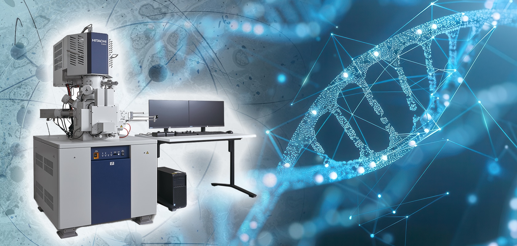
Electron microscopes use electron beam, which is shorter in wavelength than light, to visualize even the most minute structures not visible through optical microscopes. They allow us to observe a wide range of materials, from metals and ceramics to biological tissue, making them an indispensable tool in corporate manufacturing and R&D departments, universities, and other research and medical institutions.
Hitachi High-Tech has been engaged in research and development of electron microscopes for over 80 years. Our technology and expertise have helped give rise to innovative breakthroughs in a wide variety of settings, from semiconductor manufacturing, where we are seeing on-going advancements in nanoscale miniaturization techniques, to understanding unknown viruses and formulating new drugs in the field of life sciences.
In response to global issues such as climate change, the development of new materials that can contribute to carbon neutrality (decarbonization) and the circular economy is also a pressing concern. Hitachi High-Tech electron microscopes are playing a part in bringing such materials to fruition.
The type of microscope most commonly used in everyday life is the optical microscope. These devices illuminate and enlarge targets for observation, but cannot be used for anything smaller than around 200 nanometers (0.2 thousandths of a millimeter), depending on the wavelength of the light.
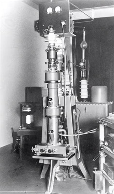
Electron microscopes, on the other hand, use electron beams with shorter wavelengths than light, enabling microscopic observations at the molecular and atomic levels. Invented in Germany in 1931, Hitachi began developing electron microscopes in the 1940s.
Shigeaki Tachibana, Chief Engineer in the CT Systems Product Division, Core Technology & Solutions Business Group, reflects on the history of Hitachi High-Tech and electron microscopes:
"Hitachi has constantly pushed the limits of performance, contributing to the evolution of various forms of research and technologies. Proving the existence of things that had been debated for a long time, such as the SEM image of the double helix structure of DNA, also strikes me as very significant."
There are two main types of electron microscopes, TEMs and SEMs, which use electron beams in different ways to observe samples. Let's take a look at their unique characteristics.
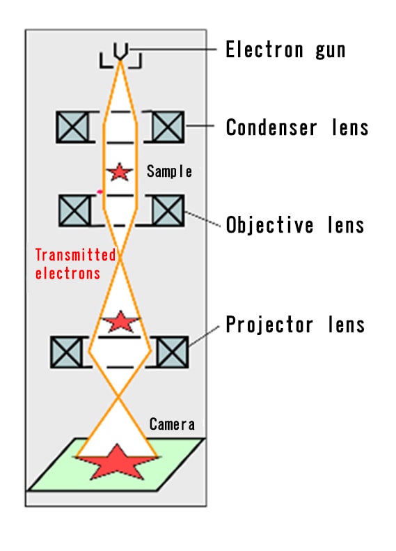
TEMs (transmission electron microscopes) irradiate the sample with an electron beam and form an image from the transmitted electrons.
The transmission rate of the electron beam changes in accordance with the structure and positioning of the sample, with these differences then captured to produce the image. The basic principle is the same as that of an optical microscope. The history of electron microscopes began with TEMs.
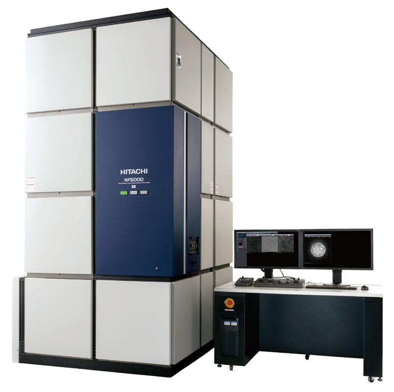
"Resolution" is an indicator of the electron microscope's capability to measure or identify targets, and Hitachi High-Tech TEMs have achieved a resolution of 0.078 nanometers (78 picometers *7, *8), the highest in the world, for observing both static and moving images.
The diameter of a single atom, the smallest unit of matter, is approximately 0.1 nanometers. With a resolution surpassing this and high elemental mapping performance, TEMs are indispensable for the development of new materials in the field of nanotechnology, as well as for structural analysis in the field of life sciences.
To make observations using TEMs, samples must first be thinned into laminates so that electrons can transmit through them to form an image. By automating this process, Hitachi High-Tech has significantly reduced the time and effort required to complete this step.
On the other hand, SEMs (scanning electron microscopes) use a narrow-focused electron beam to scan the sample in two dimensions, detecting signals generated from the areas struck by the electron beam to create an image. Detailed information on the shape and composition of the sample can be obtained from the signal type.

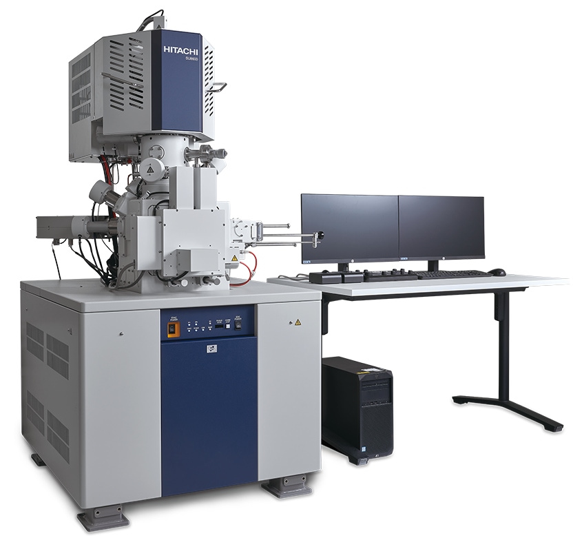
SEMs can also be combined with other analyzers to identify the elements contained within a sample based on signal type. These characteristics are used in semiconductor defect analysis and a range of other applications.
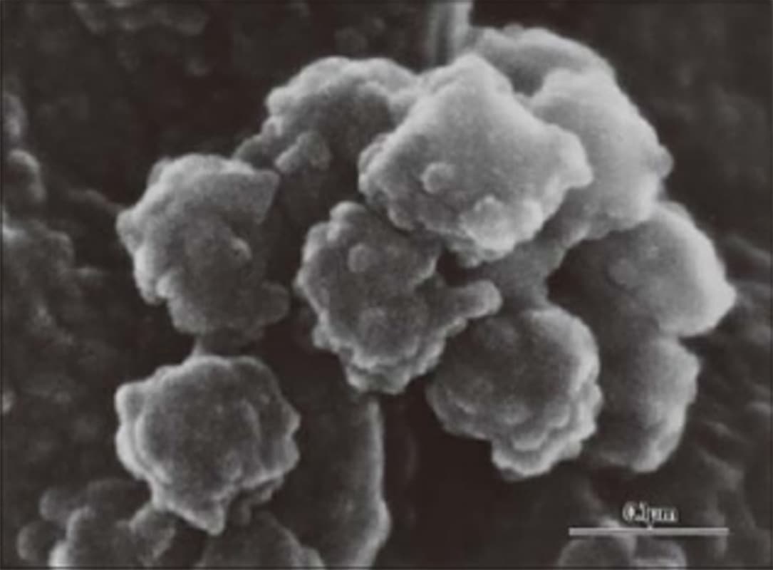
The resolution of SEMs is not as high as TEMs, but they can be used to observe small objects without the need for additional processing. This distinctive trait is what enabled us to observe stereoscopic images of the AIDS virus and double helix structure of DNA, as mentioned above.
The turning point in the evolution of Hitachi High-Tech's SEMs was the launch of the field emission SEM (FE-SEM) in 1972. One of the factors that determines resolution is brightness of the electron beam. This was increased 1000-fold for the FE-SEM compared to conventional SEMs, drastically improving its observational capabilities.
The performance of the objective lens that focuses an electron beam onto the sample also affects the resolution. Hitachi High-Tech's SEMs developed the "In Lens" system, which helps to minimize aberration (blurring and distortion).
Hitachi High-Tech electron microscopes equipped with these core technologies are supporting the development of society in a diverse range of scenarios.
One field in which Hitachi High-Tech electron microscopes play an active role is semiconductor manufacturing. Semiconductor devices are essential for key components of the digital society, including generative AI (artificial intelligence) and cloud computing, and are becoming increasingly fast with higher performance and lower power consumption with each development iteration.
Semiconductor devices, used in conjunction with ICs (integrated circuits) and LSI (large-scale integration), form electrical circuits consisting of transistors and wires on silicon wafers. As miniaturization (reduction in the scale of devices) progresses in step with performance advancements, it is no exaggeration to say that research and development and quality control of semiconductors are now reliant on electron microscopes.
"As an example, modern smartphones have more than 10 billion transistors on a chip of one square centimeter," explains Akira Ikeuchi, Assistant Manager in the Global Sales Planning Department, CT Systems Sales Division.
"The distance between transistors is on the scale of nanometers, and device structures are becoming more three-dimensional. Electron microscopes are used in a variety of applications, including the development of devices, checking for dimensional errors in finished products and analyzing the causes of faults in defective products."
In 1984, Hitachi High-Tech launched the CD-SEM (critical dimension-scanning electron microscope) for measuring the critical dimensions of semiconductor chips. As a result, electron microscopes, which until then had primarily been used in research institutions such as universities and medical institutions, made their way into mass-production manufacturing.
Today, as Mr. Ikeuchi explained, their applications throughout the manufacturing process are expanding. For example, in the event of micro-defects, it is common to use SEMs, which can observe wide areas, to determine the approximate location, and then TEMs, which boast higher resolutions, to pinpoint the exact location of the defect.
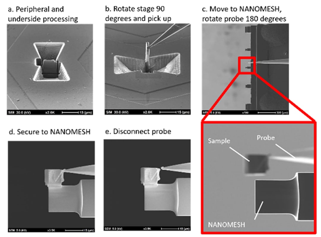
As previously mentioned, in the case of TEM observations, samples must first be thinned so that electron beams can pass through them. However, this requires the manual operation of skilled technicians and has proved something of a bottleneck in terms of improving the accuracy and speed of defect analysis.
As a solution, Hitachi High-Tech offers automated Micro-sampling. SEMs are combined with FIB *9 processing technology to process samples into lamella of only a few square micrometers in size. The process of attaching the thinned samples onto the specimen carrier for TEM observation has also been automated, simplifying the workflow for less experienced technicians.
Electron microscopes are actively used primarily in three areas of life sciences: 1) basic research in fields of medical sciences, biology and pharmaceuticals; 2) histopathological analysis and diagnosis; and 3) elucidation of unknown viruses and infectious diseases.
An example of an application in basic research is in the "discoveries of the mechanisms of autophagy" that won the Nobel Prize in Physiology or Medicine in 2016. The study in question was carried out by Yoshinori Ohsumi, Professor Emeritus of the Tokyo Institute of Technology (now the Institute of Science Tokyo).
Autophagy is the process in which cells break down and recycle intracellular components in order to maintain themselves healthy, and contributes to health and longevity.
Hitachi High-Tech's TEM was used as the means by which to elucidate this mechanism. TEM images showing how cytoplasm is taken into vacuoles and broken down were observed, which aided understanding of the autophagy process.
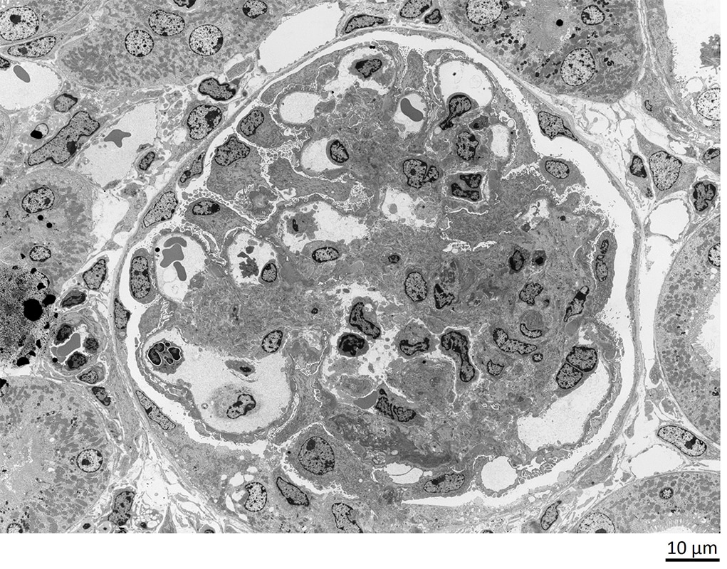
One example of how electron microscopes are used for histopathological analyses is kidney disease. It is considered difficult to identify kidney disease due to the kidney's complex structure and the fact that symptoms tend not to appear until the disease worsens, making it difficult to classify.
Basically, TEM observation can help to diagnose the disease by identifying deposits in the kidney glomerulus and subtle structural changes to basement membranes, etc.
In addition, Hitachi High-Tech has begun attempting to apply low-vacuum tabletop SEMs to pathological diagnosis. Because tabletop SEMs are easy to handle, it is expected that they will be able to help reduce the burden on medical institutions and also improve QoL (quality of life) for patients by making it possible to quickly diagnose diseases, decide on treatment plans and determine prognosis.
The COVID-19 pandemic that occurred in 2020 reaffirmed the importance of preparing for unknown viruses and infectious diseases. In the event of a new infectious disease or bioterrorism outbreak, electron microscopes will be required to identify and analyze pathogens.
Drug-resistant bacteria are also a global threat. In 2021, Hitachi High-Tech, in collaboration with a French research institute, developed a method to determine drug resistance in just one to two hours, as opposed to the usual 24 hours. SEMs were used in the research that led to this breakthrough.
Marina Wayama, Assistant Manager in the Global Sales Planning Department, Beam Technology & Analytical Systems Business Division, explains that further improvements to usability are needed:
"In the life sciences field, the number of trained people who can handle electron microscopes has been decreasing in recent years due to retirement and other factors. There's also a demand to dedicate precious human resources and time to research activities as the primary focus, rather than operating equipment. Ideally, what people want are devices that automatically observe and acquire data without the need for any human intervention."
Hitachi High-Tech Group has formulated five materialities (key topics) for solving social issues, based on SDGs (sustainable development goals).
Electron microscopes support battery production sites, helping achieve: "1: Contributing to a Sustainable Global Environment," "2: Contributing to Healthy, Safe, Secure Lives" and "3: Contributing to the Sustained Development of Science and Industry."
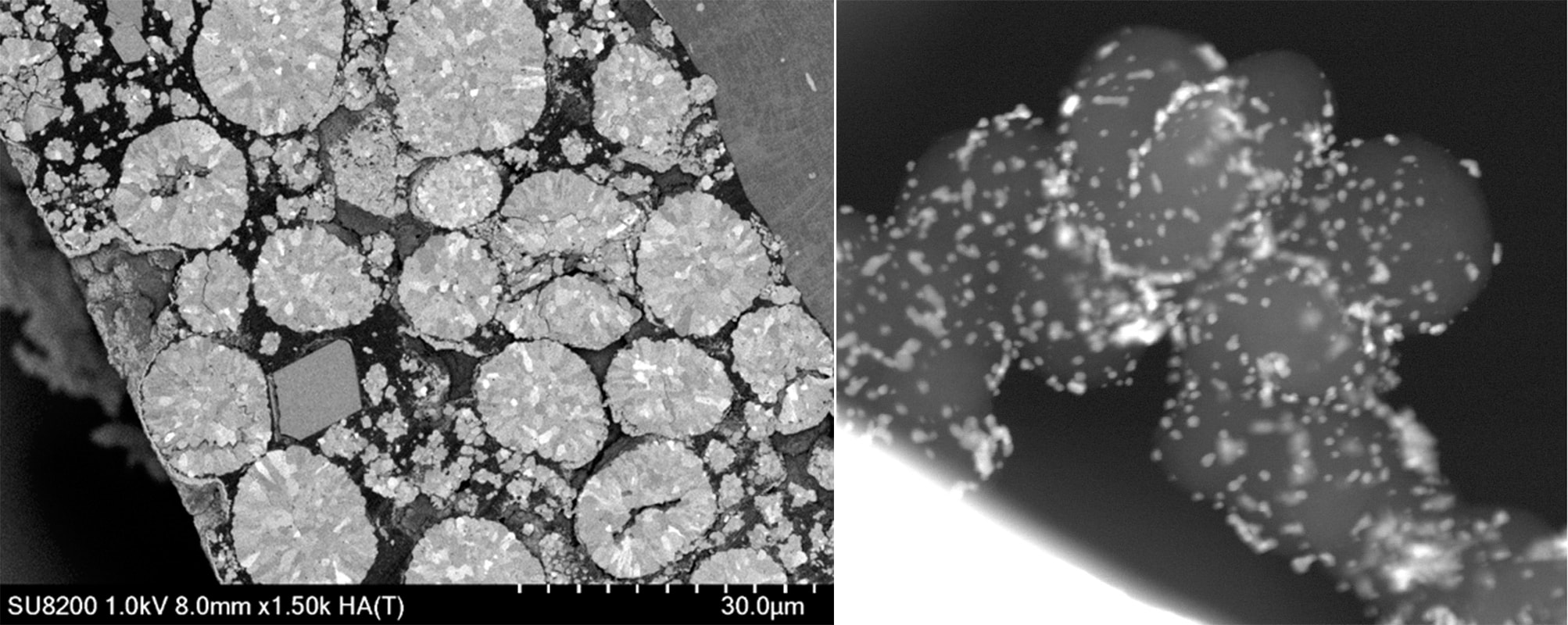
As an example of Materiality 1, "Contributing to a Sustainable Global Environment," SEMs are used in the development and manufacturing of lithium-ion batteries. These batteries are an essential device in expanding the use of EVs (electric vehicles) and renewable energy, and their demand will only continue to grow.
In order to transition to a carbon-neutral and recycling-oriented society, the development of new materials to replace conventional metals and plastics is also required. TEMs are used to observe and analyze catalysts (substances that promote chemical reactions), one of the technologies underpinning this.
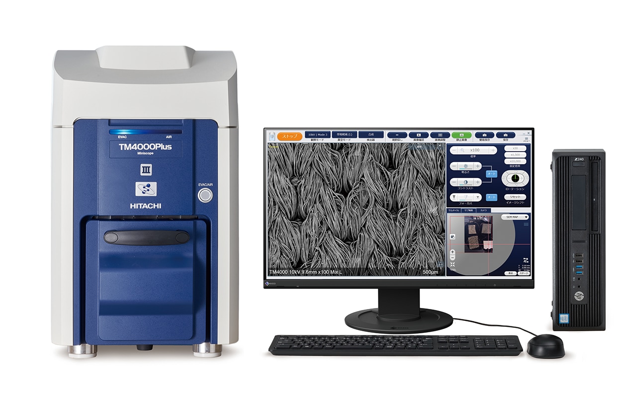
One of the pillars of Materiality 3, "Contributing to the Sustained Development of Science and Industry," is contributing to the development of the next generation of human resources. As part of this, we are working to support science education by lending models of the tabletop SEM called the "Miniscope" to schools.
Akira Ikeuchi, Assistant Manager in the Global Sales Planning Department, CT Systems Sales Division, looks forward to what the future holds:
"Human anatomy diagrams in encyclopedias used to be illustrations, but these days real images taken with electron microscopes are used instead. When I visited a classroom to give a guest class as part of our science education support activities, there were kids whose eyes lit up when they examined their own hair under a microscope. I'm glad electron microscopes are helping to create opportunities for the next generation to become interested in science and chemistry, as they're the ones who will drive innovation in future."
Our electron microscopes, which utilize electron beams, one of our core technologies, will continue to help resolve social issues and contribute to achieving a sustainable society through observation, measurement and analysis.