
Hiroyuki Shinada
PhD, Principal Researche
Basic Research Center
Research and Development Group
Hitachi, Ltd.
Member, Japanese Society of Microscopy
Member, Japan Society of Applied Physics
Member, Society of Instrument and Control Engineers
The development of novel materials with revolutionary new properties and functionality requires measurements—with atomic-scale resolution—of the electromagnetic fields inside those materials, clarifying the quantum-mechanical phenomena responsible for material properties and functionality. To enable these investigations, we have developed a powerful tool: an ultra-high-voltage (1.2 MV) holography electron microscope.
The holography electron microscope is a measurement instrument whose first successful practical application was achieved in 1978 by Dr. Akira Tonomura using a field-emission electron gun.1,2) The accelerating voltage was subsequently increased to achieve higher resolution and to allow observations on thicker samples. In 2000, Hitachi and the university of Tokyo jointly developed the world's first ultra-high-voltage (1 MV) holography electron microscope3) and used it to help clarify the superconductivity mechanism in high-temperature superconducting oxides.4) The 10+ years since that breakthrough have witnessed major progress in the technology surrounding electron microscopy, and we have now exploited those technical advances to develop the ultimate holography electron microscope, achieving the world's highest resolution of 43 pm. This report surveys the development of this instrument.
As shown in the schematic diagram in Figure 1, the atomic-resolution holography electron microscope is equipped with three tanks, in which are installed a 1.2 MV high-voltage generating circuit, a power supply for electron-gun control, and an electron gun and accelerator tube. Because high voltages (minus 1.2 MV) are applied to these pieces of equipment, they are stored in tanks filled with SF6 (sulfur hexafluoride) gas to prevent electrical discharge. In addition, the high-voltage power supply is installed at a location separated from the main unit of the electron microscope to reduce the influence of the various types of noise it emits; the supply is connected to the main unit by a high-voltage cable. This basic structure is similar to that of the 1 MV ultra-high-voltage holography electron microscope completed in 2000;3) however, to achieve the significantly increased resolution of the present instrument required overcoming four major technical challenges, as discussed below.
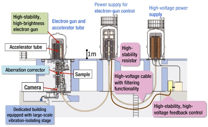
Fig.1 Overview of atomic-resolution holography electron microscope.
This is a 1.2 MV ultra-high-voltage electron microscope using a three-tank scheme in which the high-voltage power supply is separated from the main unit in order to achieve high stability. The tanks are interconnected by high-voltage cables.
Optical microscopes use a combination of convex and concave lenses to correct spherical aberration in lenses. In electron microscopes, on the other hand, for many years it was not possible to exploit the functionality of concave lenses, and improvements in resolution were thus constrained by spherical aberration. Devices for correcting such aberration became available for practical use in 1995,5) but extracting good performance from these devices required high stability from the electron microscope units on which they were mounted, and for this reason they were not installed on large-scale ultra-high-voltage electron microscopes. By surmounting the technical challenges described below to yield significant improvements in equipment stability, we succeeded in mounting a spherical aberration corrector on an ultra-high-voltage electron microscope for the first time in the world.
Energy fluctuations in an electron beam cause defocusing even in the presence of a spherical aberration corrector. For this reason, it is essential that an exceedingly stable voltage be used to accelerate the electron beam. Calculations indicated that, to attain a target resolution on the order of 40 pm, energy fluctuations in the electron beam would need to be kept below 0.6 eV while maintaining the high energy of 1.2 MeV. To improve the stability of the voltage used to accelerate the electron beam, we developed low-noise resistors with low temperature coefficients and a high-voltage cable equipped with noise-filtering capabilities. The 1.2 MV ultra-high-voltage power-supply system we developed boasted a stability of 3×10⁻⁷, approximately 70% greater than the stability of previous systems.
In the 1 MV ultra-high-voltage electron microscope and other typical field-emission electron guns, a voltage (the extraction voltage) is applied to extract electrons, and the emitted electron current begins to decrease immediately after the start of electron emission. For this reason, when using machines of this type the extraction voltage must be adjusted once or twice per day. However, the trajectory of the electron beam shifts—if only slightly—each time the extraction voltage is adjusted, and for this reason it is not easy to operate the spherical aberration corrector under optimal optical-axis conditions. We felt that we needed a field-emission electron gun that could be used without adjustment throughout a full day's observations. Although high-stability field-emission electron guns have been increasingly used for practical applications in recent years, we needed to advance this technology further, increasing the strength of the vacuum inside the electron gun to several times that found in the newest models; ultimately we developed an electron gun with an interior vacuum strength of 3×10⁻¹⁰ Pa (Pascals), some 100 times stronger than that for the 1 MV microscope developed in 2000 (Fig. 2).8)
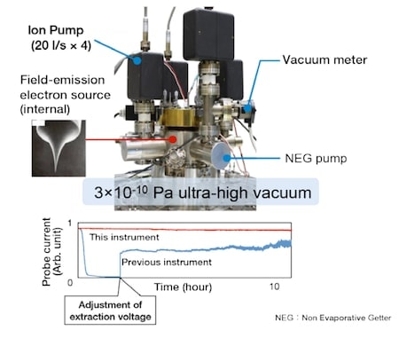
Fig.2 High-stability, high-brightness electron gun
Previous electron guns suffered from a decrease in electron emission immediately after the start of electron emission, requiring adjustment of the extraction voltage and other parameters, and consequential wait times for the system to stabilize. In this instrument, we used an ultra-high vacuum to ensure that the system is stable and ready to use from the moment of electron beam extraction.
Successful atomic-scale observations require that both the electron beam and the measurement sample be isolated from external disturbances—including vibrations, sound waves, and magnetic fields—to the greatest possible extent. To suppress the effects of such disturbances, we constructed a dedicated building for our microscope; inside the experimental chamber we installed sound absorbers and implemented a precision temperature-control system. The performance of the resulting chamber exceeded our initial objectives: sound isolation and low-noise performance of ≤20 dB (>200 Hz), floor vibrations of 7.2×10⁻⁴ cm/sec2 at 100 Hz, and temperature stability of ±0.2°C/8 hours (Fig. 3).7)
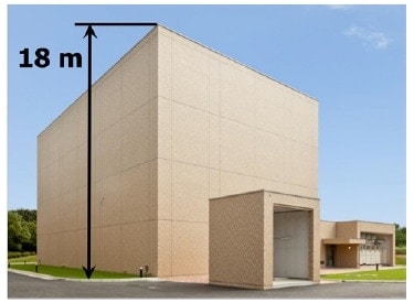
Fig.3 Electron microscope building designed to provide stable low-noise environment
High sound isolation and low-noise performance: ≤20 dB (>200 Hz)
Reduced floor vibrations: 7.2×10⁻⁴ cm/sec2 (100 Hz)
Temperature variation (room temperature) around the microscope: ±0.2°C/8 hours
The development process was beset by numerous unexpected tragedies and other difficulties. Here we touch briefly on four of these challenges that proved particularly severe.
Although the project was officially launched in March 2010, a serious setback was suffered when Isao Matsui—a veteran engineer with a long history of involvement with the development of ultra-high-voltage electron microscopes who played a key role in the project proposal—collapsed and died suddenly of scirrhous stomach cancer. Surely nobody was more deeply affected by this tragedy than Dr. Tonomura, who had worked closely with Matsui in advancing this project. Nonetheless, Dr. Tonomura's ongoing dedication to the project served as an inspiration to the remaining team members, who continued—if in a somewhat somber mood—to carry out their development efforts. Through the indefatigable efforts of the designers, the design of the major system components—including the dedicated building, the high-voltage cable, and the high-pressure tanks that housed the high-voltage equipment—proceeded on schedule, as did arrangements for their construction.
The Great Tohoku Earthquake struck in March 2011. Although the development center in Saitama prefecture suffered no major damage, the high-voltage cable, which was under construction in Ibaraki prefecture, received water damage during the ensuing tsunami (Fig. 4). Starting over from scratch with this special-purpose 12.5-cm-diameter high-voltage cable was out of the question on both scheduling and budgetary grounds. Miraculously, a spare cable—which was also under construction at the time and which managed to avoid water damage—was completed with only slight delays. Another narrowly-averted disaster involved the Miyagi Prefecture-based electronics manufacturer responsible for developing the ultra-high-stability power supplies that may be said to constitute the beating heart of this microscope. In an event of providential good fortune, the advancing tsunami stopped just short of the factory, and the power supply was delivered without incident. Less happily, it was around this time that Dr. Tonomura was diagnosed with pancreatic cancer. Still, Dr. Tonomura was in strong spirits when, immediately after his diagnosis, he announced the situation to the full team and insisted that he would return to the project following his treatment.
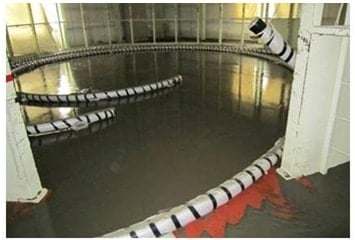
Fig.4 The high-voltage cable was damaged by the tsunami just before it was completed.
The dedicated building housing the microscope was erected in late August 2011, in accordance with the original plan (Fig. 3).7) Thereafter, the power supply and the high-voltage cable were installed, and tests involving the application of 1.2 MV high voltages were conducted in late January 2012. Unfortunately, these tests found that electrical breakdown (discharge) occurred at 900 kV (Fig. 5). Because the cable had passed high-voltage tests involving the application of 1.3 MV prior to shipment from the factory, the unexpected appearance of electrical breakdown at such a low voltage came as a major shock. A response team of in-house high-voltage experts was drafted, and a battery of investigations—including both simulations and experimental tests—revealed that, according to dynamical simulations, there were some times at which high electric fields arose in regions in which near-zero electric fields had been expected. These had been overlooked by the static simulations conducted during the design phase. New electrodes capable of withstanding increased electric fields in the problematic regions were designed, and voltage-tolerance tests were finally passed in July 2012.
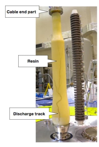
Fig.5 Electrical breakdown near the ends of high-voltage cables
A high negative voltage is applied to the tip while the base is grounded.
In experiments involving high voltages applied to the tip of the cable,
electrical breakdown occurred at voltages below the specified voltage of
1.2 MV, leaving discharge track in the resin surface.
After undergoing surgery in April 2011, Dr. Tonomura briefly recovered—to the point at which, six months after surgery, he was able to come to the laboratory—but passed away on May 2, 2012. Although this unquestionably came as a major blow to the entire team, the team had been kept informed of almost all about Dr. Tonomura's condition—at his own insistence—and were thus at least somewhat prepared for the tragic news. The question of who would succeed Dr. Tonomura as Project Leader (Principal Scientist) was a pressing problem; ultimately the project was able to continue under the leadership of Dr. Nobuyuki Osakabe, who was then Director of the Central Research Laboratory and who, in his days as a researcher, had numerous prominent accomplishments in Dr. Tonomura's research group.
By March 2014 we had progressed to the point of successfully obtaining electron microscope images with an accelerating voltage of 1.2 MV. Our next challenge was to achieve the highest resolution in the world. We had individually confirmed the stability of the high-voltage power supply, the appropriateness of the environment in which the equipment was installed, the stability of the electron beam, the operation of the aberration corrector and other components, so we felt it should be possible to achieve a resolution at the 40 pm level. In the first half of 2014 we immediately achieved resolutions of 60 pm, but subsequent progress was slow, and by October 2014 we had still not reached 50 pm. We attributed this failure to multiple factors, including the static performance of the stage, electrical noise disturbances, and sample damage. Among these, we chose to focus on sample damage in particular. To demonstrate resolution capable of identifying individual atoms, we had been observing samples that were only a few atoms thick; but subjecting such samples to continuous electron beam irradiation during observation causes their structure to collapse. For this reason, we adopted a strategy in which the focus of the electron beam would be adjusted in other locations, after which the beam would be quickly shifted to the observation site and multiple points would be imaged. As a result, we successfully observed a 44 pm spacing between Ga atoms (Fig. 6). Moreover, upon conducting resolution tests via other methods using single-crystal tungsten, we successfully captured the lattice spacing with an even better resolution of 43 pm, with good reproducibility. We announced these results in a journal article9) and were ultimately recognized as having achieved the highest resolution in the world. Figure 7 shows the principal components of the completed atomic-resolution holography electron microscope.
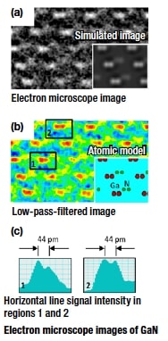
Fig.6 Observation of atomic spacing in gallium nitride (GaN).
As a demonstration of the actual resolution of the electron microscope, we successfully captured electron microscope images showing the 44-pm spacing between two gallium atoms in single-crystal gallium nitride.
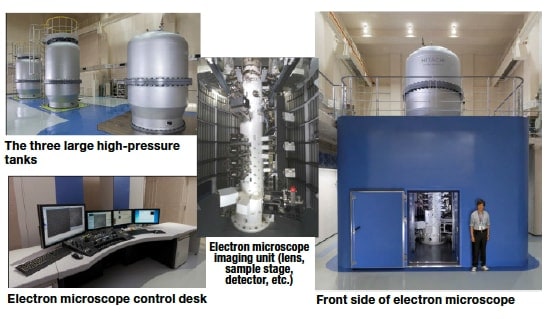
Fig.7 Atomic-resolution holography electron microscope.
The true value of this instrument lies not only in its status as the world’s highest-resolution electron microscope, but also in its ability to make quantitative measurements of electromagnetic fields with atomic-scale resolution. By making full use of the power of this instrument to understand the quantum-mechanical phenomena responsible for the functionality and properties of highly functional material such as magnets, batteries, and superconductors, we hope our instrument will contribute to the advancement of basic science through research and development involving revolutionary cutting-edge functional materials.
This development project was supported, through the Japan Society for the Promotion of Science, by the Funding Program for World-Leading Innovative R&D on Science and Technology, established by Council for Science, Technology, and Innovation.
References
See more