Takehiro Yamaoka*1, Yuta Seki*2
At Hitachi High-Tech and Hitachi High-Tech Science, we develop, manufacture, and sell a wide range of analytical instruments to support research and development for lithium-ion batteries (LIBs); these instruments include scanning electron microscopy (SEM), atomic force microscopy (AFM), and X-ray impurity analysis systems for use in quality control. In this article we first present experimental case studies illustrating the use of SEM, AFM, and X-ray impurity analysis to characterize conventional liquid-electrolyte-based LIBs, and then discuss our ongoing efforts to apply these methods to the study of all-solid-state LIBs.
Approaches to SEM characterization of LIBs span a wide gamut of techniques, but most methods focus on the outermost sample surface or on cross sections, investigating properties such as the microscopic structure, material composition, and electrostatic potential distribution via low-acceleration, high-magnification field-emission SEM (FESEM). The use of electron energy-loss spectroscopy (EELS) together with transmission electron microscopy (TEM) yields information on active materials and chemical bonding states at sample surfaces. Efforts to address the problem of increased internal resistance in LIBs have made use of scanning spreading resistance microscopy (SSRM)—a type of AFM—to characterize the resistance distribution in various materials subjected to kneading processes, as well as variations in the resistance distribution before and after charge-discharge cycling.
Figure 1 is a conceptual diagram illustrating how SEM, AFM, and ion-milling systems developed by Hitachi High-Tech may be interconnected in an air-protected configuration. The sample is mounted in an air-protected sample holder with a sealing cap. When we wish to use a particular instrument to process, analyze, or observe the sample, we insert the sample holder into the instrument’s transfer vessel, and only then do we open the cap to expose the sample inside the instrument. After processing or measurement, the cap is re-sealed and the sample holder is transferred to
the next instrument. At Hitachi High-Tech, we have introduced the term SÆMic1). to describe correlative SEM/AFM microscopy; in what follows, we will refer to the setup shown in Figure 1 as our air-protected SÆMic (AP-SÆMic) system. The AP-SÆMic approach enables correlative analyses in which multiple instruments are used to analyze the same microscopic region of a single sample, simultaneously yielding information on sample structure and composition, elemental mapping, 3D morphology, resistance distributions, electric potential distributions, and other properties.
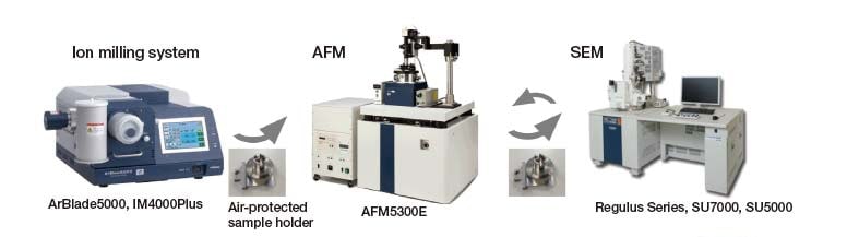
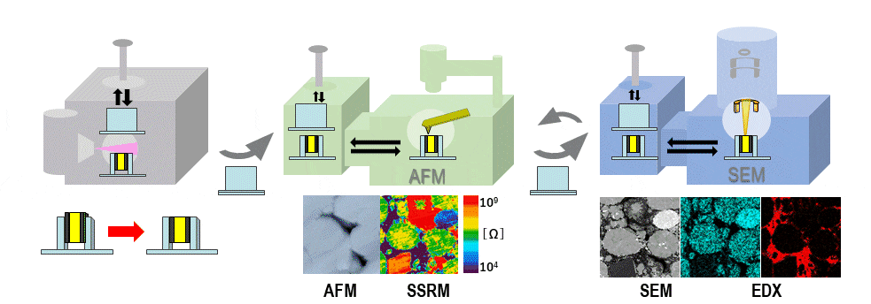
Fig. 1 Air-protected SEM/AFM/ion milling system.
Figure 2 shows SEM images of a cross-sectional sample of an LIB anode after charging, as observed before (left) and after (right) exposure to the ambient environment. Figure 2(a) is an SEM image following cross-sectional ionmilling with the sample maintained in an air-protected state throughout2); note that the internal structure of particles of graphite—the anode active material—is clearly visible. Figure 2(b) is an SEM image of the same sample region after exposure to air for 15 minutes; evidently the surface configuration is drastically altered. This is due to extensive transformation of the surface of highly reactive materials containing Li ions when exposed to adsorbed water, moisture, oxygen, or other reactive substances. As this example demonstrates, for analysis of the LIB microstructure, it is essential to keep samples air-protected throughout cross-sectional processing and observation.
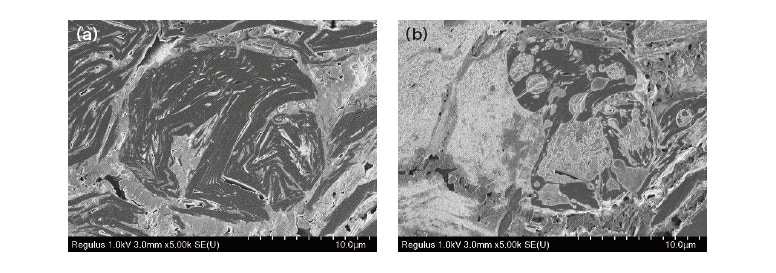
Fig. 2 SEM observations of cross-sectional sample of LIB anode after charging. (a) Sample as maintained in air-protected state. (b)Sample after exposure to air.
Charge-discharge cycle tests to analyze the degradation mechanism are essential for enhancing the performance and extending the lifetime of LIBs. In Figure 3 we present the results of an AP-SÆMic correlative analysis to characterize the impact of charge-discharge cycling for an LIB anode made from a mixture of Si and graphite3). The figure shows SEM-EDX structural analysis results, elemental mapping data, and SSRM results for the electrical resistance distribution observed (a) before cycle tests (left), (b) after cycle tests at room temperature (center), and (c) after cycle tests at high temperature (right). Note that, in the SSRM image of the sample before cycle tests, graphite-based activematerial boundaries are generally low-resistance regions; in contrast, the SSRM images of the sample after roomtemperature or high-temperature cycling indicate that these boundaries have become high-resistance regions. Beneath each SSRM image we have plotted the spatial variation of the electrical resistance along the line segments indicated in blue within the images. Before cycling, the electrical resistance decreases by approximately one order of magnitude at graphite-based active-material boundaries compared to that within the particles. In contrast, after room-temperature cycling the resistance at the boundaries increases by 2 to 3 orders of magnitude. Moreover, after high-temperature cycling the high-resistance regions between graphite-based active-material particles extends throughout the plane of the sample. The increased concentration of fluorine (F) observed post-cycling at the boundaries between graphite-based and Si-based active-material regions suggests the formation of a solid-electrolyte interface in these regions, explaining the increase in electrical resistance. The lowest resistance is observed for the Cu foil that serves as the current collector.
The label (A) in Figure 3(b) indicates a graphite-based active-material region that is identical to other active-material regions—as confirmed by SEM-EDX elemental-mapping results—but whose electrical resistance after room-temperature cycling is an order of magnitude larger than that of other active-material regions. This is presumably one reason for the increase in the internal resistance of LIBs. Similarly, around the perimeter of the Si-based active-material region labeled (B) in Figure 3(c), after high-temperature cycling, a clearly discernible distribution of F with concentrations even higher than those observed for graphite-based active-material regions is seen; a high electrical resistance is also present throughout Si-based active-material regions. Also, although not shown in Figure 3, the results of EDX elemental analysis after high-temperature cycling indicate the presence of phosphorus (P) at and near the boundaries of Si-based active-material regions. This phosphorus is not among the constituent elements of the original anode material, but rather originates from the electrolytic solution; its presence is indicative of corrosion caused by reactions between Si and the electrolyte induced by charge-discharge cycling. This example demonstrates the wealth of insights that may be gleaned from AP-SÆMic analyses involving SEM-EDX and SSRM characterization of identical sample regions.
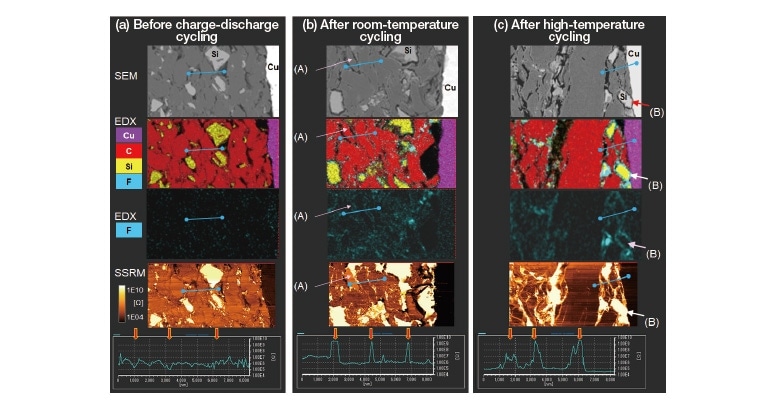
Fig. 3 SSRM profiles for graphite-based active-material regions before and after charge-discharge cycling. (Arrows indicate electrical resistance at graphite-based active-material boundaries.)
Source: Taken, with modifications, from Hitachi High-Tech Application Datasheet HTD-AFM-035.
Figure 4 shows the EA8000A X-ray impurity analyzer—an instrument that combines transmission X-ray imaging with X-ray fluorescence analysis—with a schematic diagram illustrating the mechanism of impurity detection. The EA8000A is capable not only of rapidly scanning large sample regions—up to 250 × 200 mm—to detect metallic impurity particles with sizes of 20 μm or larger, but also boasts the ability to perform high-speed sequential composition analyses, making it an essential tool for LIB quality control. The transmission X-ray imaging system that detects metallic impurities consists of an imaging sensor and an X-ray tube positioned above and below the sample, respectively; the position coordinates of impurity particles detected by this system are passed on to an X-ray fluorescence analyzer, which conducts fluorescent X-ray elemental-mapping analysis at those coordinates to identify the elemental composition of the impurity. The X-ray fluorescence analyzer uses a polycapillary to capture primary X-rays emitted from the X-ray tube. Irradiating microscopic sample regions with high-intensity X-rays allows rapid identification of the elemental composition of such impurity particles embedded in the interior of samples.
When the raw materials used to fabricate LIBs are contaminated by metallic impurities, the impurities cannot be removed at later processing stages and are one of the main sources of defects and malfunctions in fabricated devices. For this reason, it is essential to screen for metallic impurities at the raw-material stage. However, X-ray impurity analysis cannot be used directly for this purpose, because the nature of the raw materials makes them susceptible to X-ray damage. This creates a need for preprocessing techniques such as removal by magnetic selection or vibrational sorting—which, however, are themselves problematic. Magnetic selection may fail to remove non-magnetic impurities, while vibrational sorting is an inefficient process requiring large amounts of time to handle significant quantities of raw materials.
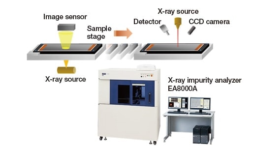
Fig. 4 Overview of EA8000A X-ray impurity analyzer
Instead, we turn to an alternative method that is capable of detecting non-magnetic impurities and can handle large quantities of raw materials: the spin-air-sieve approach for particle-size analysis, developed by Seishin Enterprise, in which circulating air currents are used to sort particles. As we now demonstrate, this approach—in combination with the high-speed impurity analysis capabilities of the EA8000A—yields a technique that enables high-throughput screening for metallic impurities in the raw materials used to prepare cathode active materials. The basic process is outlined in Figure 5. The residual substances that remain after the desired particles have been selected may be recovered simply by using a special adhesive film designed for use with the EA8000A, eliminating the need for complex or unwieldy sample preparation procedures. This method offers an extremely efficient way to screen for metallic impurities in cathode active materials—a problem for which no effective solution had previously been established—and will be of enormous utility in screening raw materials upon shipping and upon delivery.
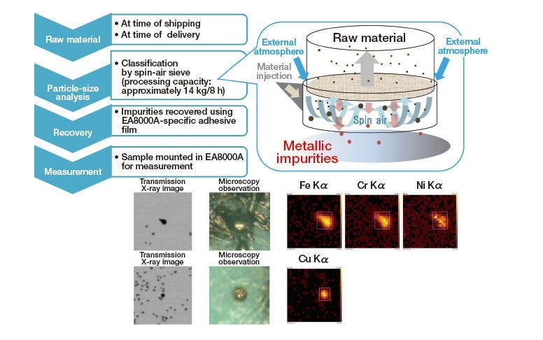
Fig. 5 Outline of accelerated particle-size-analysis preprocessing technique that enables rapid screening of microscopic metallic impurities. The inset is a conceptual diagram illustrating the spin-air sieve technique for rapidly detecting microscopic metallic impurities.
In recent years, industry has expressed increasingly high hopes for the development of all-solid-state LIBs, in which the organic liquid electrolytes of conventional LIBs are replaced by inorganic solid electrolytes. However, one disadvantage of all-solid-state LIBs is that their solid-solid contact interfaces and interfacial reaction layers pose barriers to ionic and electronic conduction, thus increasing the internal resistance. Consequently, the establishment of interfacial control strategies for reducing interfacial resistance—and the development of techniques for analyzing these strategies—have become an urgent priority.
Figure 6 shows results of a correlative AP-SÆMic analysis of an all-solid-state LIB in which the solid-electrolyte (SE) material is 75Li2S∙25P2S5 (LPS) 4). In this analysis, the sample is a composite cathode layer on a cross section of the LIB after initial charging, and we observe the microscopic structure, surface potential, and resistance distribution in a single sample region. For a detailed discussion of the correlations among the various components of this analysis, we refer the reader to Ref. 5. The SSRM image shows a sea of high-resistance SE material in which is embedded a chain of NMC particles with distinct resistance values, responsible for mediating electronic conduction. However, the resistance of the NMC particles indicated by arrows is greater than that of other NMC particles, which may lead to increased internal resistance and degraded battery performance. By conducting AP-SÆMic analyses before and after charging, we can investigate correlations among phenomena associated with charging reactions, including variations in electrical resistance and surface potential5).
In addition to the work presented here, we also pursuing the use of TEM techniques for in-situ observation of phenomena such as reactions with environmental gases that degrade the performance of sulfide-based all-solidstate LIBs, as well as changes in solid-electrolyte crystal structures under heat treatment6). Also, in this article we discussed X-ray impurity analysis as a technique for detecting impurities in LIB materials, but an alternative approach is to combine coherence scanning (white-light interferometric) microscopy—a technique allowing high-speed, highprecision
measurements of 3D morphologies—with SEM-EDX analysis of identical sample regions. This approach is especially promising for determining the impurity composition in LIBs and controlling the sizes of individual constituent particles. Going forward, Hitachi High-Tech will continue to pioneer novel combinations of observational and analytical techniques to deliver comprehensive solutions for LIB analysis.
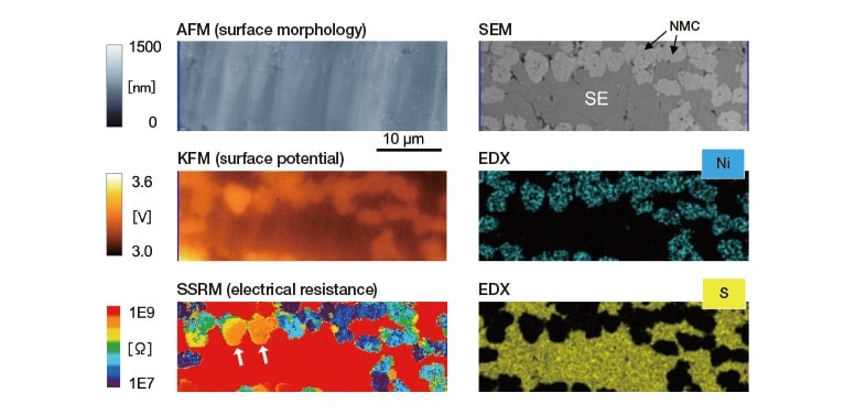
Fig. 6 AP-SÆMic analysis of composite cathode layer in sulfide-based all-solid-state LIB.
Source: Taken, with modifications, from Hitachi High-Tech Application Datasheet HTD-AFM-041.
Acknowledgements
We are grateful to Seishin Enterprise for invaluable assistance with spin-air sieves for particle-size analysis in the preparation of cathode active materials. For provision of all-solid-state battery samples, and for valuable discussions on AP-SÆMic experiments, we are grateful to Dr. Misae Otoyama (currently at AIST), Associate Professor Atsushi Sakuda, and Professor Akitoshi Hayashi of Osaka Prefecture University.
References
Publication data
Published in the monthly journal Engineering Materials (April issue 2021).
About the authors
Analysis Systems Solution Development Department
Metrology and Analysis Systems Product Division
Nano-Technology Solution Business Group
Hitachi High-Tech Corporation
Application Development Center
Hitachi High-Tech Science Corporation
