Shigeaki Tachibana
Field-emission scanning electron microscopy (FE-SEM) has been used in a wide range of fields such as nanotechnology, semiconductors, electronics, life science, and materials because of its high resolution images, rich information, and relatively easy handling of specimens. In recent years, the use of FE-SEM for materials integration and other purposes spanning an increasingly diverse spectrum of research disciplines has created a demand for new techniques capable of acquiring large quantities of data in shorter periods of time with less user effort.
To address these needs, in December 2021 Hitachi High-Tech released two new instruments—the SU8600 and SU8700—that combine high-resolution FE-SEM performance with enhanced automation capabilities supporting highvolume data acquisition.
As data-driven research and development styles—which, by definition, require large quantities of input data— become increasingly ubiquitous in the years to come, these instruments will allow rapid acquisition of large datasets while streamlining operation for users.
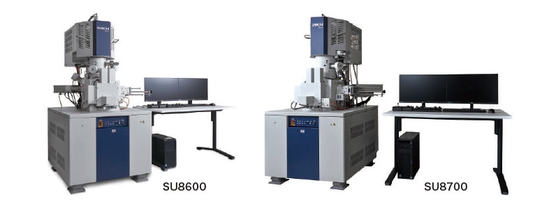
Fig. 1 SU8600 (left) and SU8700 (right).
In FE-SEM observation and analysis, the electron optical system must be adjusted each time in order to set the measurement conditions according to the specimen and purpose. The time required for this adjustment is highly dependent on the user's skill level, and is one of the factors causing variations in data quality and instrument throughput. The SU8600 and SU8700 are equipped with a function that automates the alignment of the electron optics, enabling stable setting of optical conditions.
As instruments grow more sophisticated over time, they deliver larger and larger datasets of greater and greater complexity, and the task of manually acquiring such large, complicated datasets becomes increasingly burdensome to users. The SU8600 and SU8700 feature an optional tool known as EM Flow Creator that helps users create their own recipes for automated data acquisition based on user-specific data-acquisition conditions. For example, a sequential data-acquisition recipe might switch detectors at arbitrary locations before acquiring images. Creating homemade recipes in accordance with given measurement objectives affords extensive freedom in the design of automated dataacquisition schemes.
The enhanced SEM functionality and improved instrument performance of the SU8600 and SU8700 ensure that these instruments offer a broader variety of data outputs as well. In an attempt to display as much of this information as possible, the SU8600 and SU8700 feature improved display capabilities, including the following:
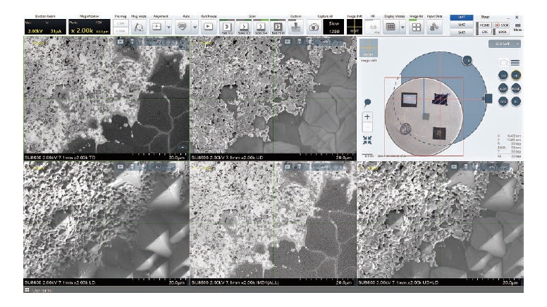
Fig. 2 SU8600 control screen simultaneously displaying images from multiple detectors (5 detector channels) plus cameranavigation image. (Specimen: Solar cell.)
The left image in Figure 3 was taken with 40,960 × 30,720 pixels, and the right image is a digital enlargement of the yellow square of the left image. Despite the large area covered by the saved image—approximately 120 μm width—the image quality in the digital enlargement is sufficient to reveal nerve-cell organelles and other interior structures.
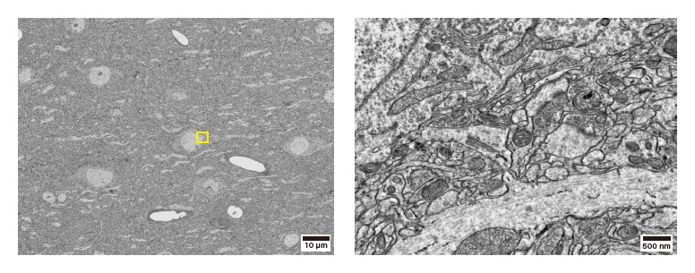
Fig. 3 High-definition image of rat cerebral cortex. (Image captured with SU8700.) Specimen courtesy of Dr. Yoshiyuki Kubota, Section of Electron Microscopy, National Institute for Physiological Sciences
Emitter brightness is important for observations at low accelerating voltage. The SU8600 incorporates a highbrightness cold-field emitter (CFE) to allow acquisition of ultra-high-resolution images even at low accelerating voltages.
The use of an ExB field—which can detect signals with high efficiency— inside the column allows high-efficiency signal detection. This is useful for high-resolution observations in particular at short working distances.
The SU8600 has an enhanced detector option to capture as many of the various signals emitted from the specimen during SEM observation as possible:
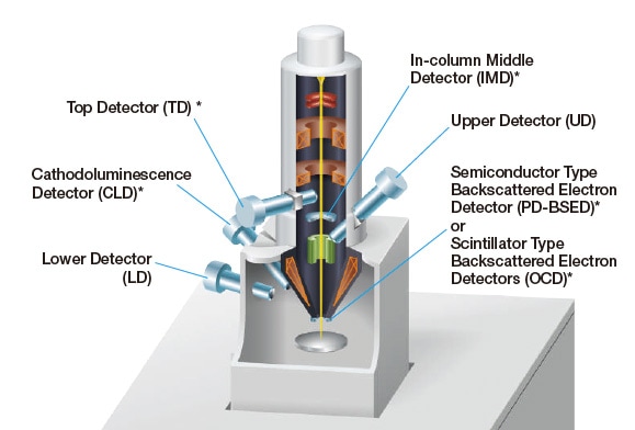
Fig. 4 SU8600: Cross-sectional diagram of column and detector configuration. Asterisks indicate optional detectors.
In observations using the newly developed Scintillator type backscattered electron detector (OCD), the faster response of the detector makes it easy to identify specific observation regions. For example, although the image in Figure 5 was acquired with an acquisition time of less than 1 second, lower-layer SRAM interconnects and Fin-FET structures are clearly discernible in the image.
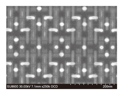
Fig. 5 Observation of lower-layer interconnects of 5 nm process SRAM.
Schottky emitters offer high brightness—close to the brightness of CFEs—as well as high probe current and high current stability. The use of a Schottky emitter for the SU8700 electron gun enables the following features:
The SU8700 allows accelerating voltage settings as low as 100 V with no bias voltage applied to the specimen stage. This allows observations at ultra-low accelerating voltages in situations where applying stage biases is difficult— perhaps for reasons involving specimen morphology.
To improve throughput, the optics and detection system of the SU8700 were designed to allow all detectors to acquire signals at the same working distance (6 mm). EDS can also be measured at this working distance, allowing all observations and analyses to be performed at the same working distance.
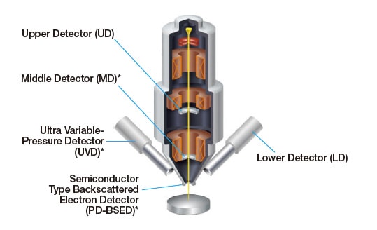
Fig. 6 SU8700: Cross-sectional diagram of column and detector configuration. Asterisks indicate optional detectors.
Figure 7 shows secondary electron (left) and backscattered electron (right) images of a tempered martensite steel specimen. In the secondary electron image, the distribution of precipitates is visible with high contrast. In the backscattered electron image, acquired under identical conditions, channeling contrast provides information of grain size and deformation.
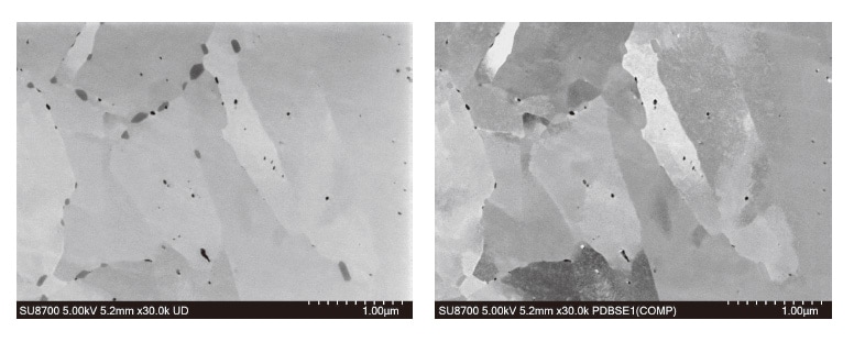
Fig. 7 The SU-8700 detector system allows multiple types of data to be acquired for the same field of view, such as the secondary electron image (left) and backscattered-electron image (right) shown here for a tempered martensite steel specimen.
Specimen courtesy of Dr. Shoichi Nambu, The University of Tokyo
The SU8600 and SU8700 FE-SEM systems feature innovative optics and detection systems whose key features allow these instruments to handle more data than ever before—while expanding imaging capability and analytical methods they support. Both systems feature enhanced automation features for adjusting optical conditions and collecting data, helping users acquire large, complex datasets and supporting the types of analytical operations that will be in ever-higher demand in the years to come.
About the author
Shigeaki Tachibana
Business Planning for Beam Technology Systems Department,
Beam Technology Systems Business Division,
Core Technology & Solutions Business Group
Hitachi High-Tech Corporation
