Takehiro Yamaoka (Analytical Application Engineering Section Tokyo, Hitachi High-Tech Science Corporation)
SEMs are systems that offer a wide variety of information, including not only image data—such as secondary-electron images (SE images) and back-scattered-electron images (BSE images) reflecting the composition of the sample—but also data on element distributions from characteristic X-ray analysis and crystal orientation analysis from EBSD. Moreover, improvements in recent years to the performance of low-acceleration observations have allowed the collection of voltage contrast data and other qualitative information on material properties. Meanwhile, thanks to innovative new types of probes and scanning methods, SPM techniques now allow—in addition to measurements of atomic-scale morphology—studies of mechanical properties, such as viscoelasticity and friction distributions, and electromagnetic material properties, such as current distributions, surface potentials, and magnetic-field distributions. By observing a sample using both SEM and SPM—at the same area—one obtains copious quantities of correlated information on the structure, composition, and material properties of the sample. An air protection sample holder—which may be used for ion milling, FE-SEM, and SPM—has already been commercialized and used in studies of lithium-ion batteries, including SEM observations of electrode materials and SPM observations of electrical resistance distributions.1)
Electric-car motors and other technologies have created increased demand for permanent magnets, and studies of high-performance magnets that use reduced quantities of dysprosium (Dy)—or Dy-free—have become an active field of research. Figure 1 shows an example in which SEM and magnetic force microscopy (MFM, a type of SPM) were used to image—at the same area—a sample of an Nd2Fe14B magnet produced by a Dy-free thermal processing and subjected to flat milling. Because of the planar-processing ion milling, the grain-boundary structure of individual microcrystals is clearly visible. Figure 1 (c) shows a transmission and superposition of an MFM image (in which bright regions correspond to spins pointing upward in the direction of the page, while dark regions correspond to downward-pointing spins) on an SE image and a BSE image. Precision control of crystal structure and magnetic properties are highly desirable for next-generation high-performance magnets; the ability to identify the direction of magnetization and to distinguish single-domain from multi-domain regions at the level of individual crystals allows detailed consideration of the relationship between the magnetic-field distribution and the crystal grain-boundary structure and material-composition distribution.2) This sort of combined SEM-SPM observation methodology at the same area is a powerful tool not only for permanent-magnet materials, but also for studying a variety of cutting-edge materials, composite materials, and devices requiring crystal/grain-boundary control.
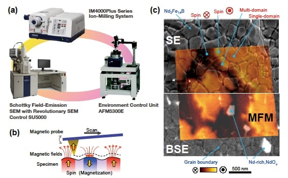
Fig.1
Observation of the nanoscale structure, composition, and material properties of a crystal/grain boundary using ion milling, SEM, and SPM at the same area
(a) The instruments used
(b) Magnetic force microscopy (MFM)
(c) Application to an Nd-Fe-B permanent magnet produced by Dy-free thermal processing
Acknowledgements
Nd2Fe14B magnets produced by dysprosium-free thermal processing were provided by Daido Steel Co., Ltd.
References
See more
