1. Semiconductor manufacturing process
A semiconductor chip is an electric circuit with many components such as transistors and wiring formed on a semiconductor wafer. An electronic device comprising numerous these components is called “integrated circuit (IC)”. The layout of the components is patterned on a photomask (reticle) by computer and projected onto a semiconductor wafer in the manufacturing processes described below.
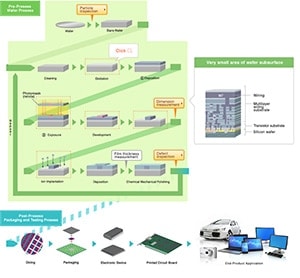
1) Wafer processing
In the manufacturing process of IC, electronic circuits with components such as transistors are formed on the surface of a silicon crystal wafer.
Basics of IC formation
- A thin film layer that will form the wiring, transistors and other components is deposited on the wafer (deposition).
- The thin film is coated with photoresist. The circuit pattern of the photomask (reticle) is then projected onto the photoresist using Photolithography technology.
- The developed photoresist is used as a mask for etching to process the thin film into the shape of the wiring and other components.
Refer to figure 2) Front-end process and back-end process.
With this, one layer of the circuit is formed. The transistors are formed on the lowest layer. Similar process is then repeated, and many layers of circuits are formed on top of one another.
Please enable JavaScript in your browser settings when using this website.
In order to read a flash file,
you need to have Adobe® Flash® Player installed in your computer.
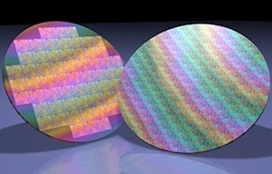
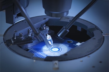
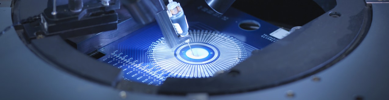
In the process of the integrated circuit creation, there are inspection and measurement steps to check whether or not the patterns are fabricated as designed. If defects are found, the fabrication will be interrupted to remove the defects from the process and to make small changes in the fabrication conditions for correction purposes. More than one hundred semiconductor dies are fabricated on a single wafer. At present, the largest silicon wafer is 300mm in diameter. Semiconductor manufacturers are looking into 450mm diameter silicon wafers for use in the future.
2) Front-end process and back-end process
Semiconductor devices are completed through the front-end process (wafer processing operation) and the back-end process (assembly process) described below.
(In the following description of the element process, a very small area of a wafer surface is magnified and shown schematically.)
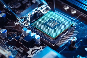
The finished semiconductor devices have been used in a variety of products such as personal computers, smartphones and cars in everyday life (see also “Semiconductors in everyday life”).
Front-end process and back-end process
Related Contents
What are semiconductors?
Semiconductor manufacturing