1. Properties of semiconductors
The name “semiconductor” is widely known, but what are semiconductors?
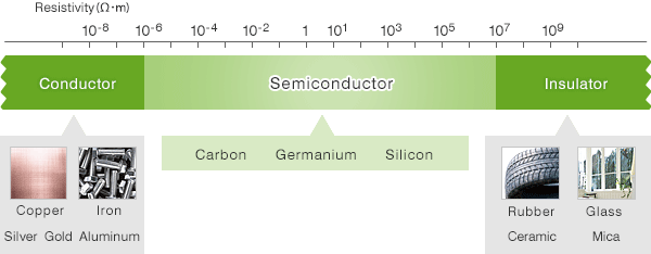
Semiconductors possess specific electrical properties. A substance that conducts electricity is called a conductor, and a substance that does not conduct electricity is called an insulator. Semiconductors are substances with properties somewhere between them.
Electrical properties can be indicated by resistivity. Conductors such as gold, silver and copper have low resistance and conduct electricity easily. Insulators such as rubber, glass and ceramics have high resistance and are difficult for electricity to pass through. Semiconductors have properties somewhere between these two. Their resistivity might change according to the temperature for example. At a low temperature, almost no electricity passes through them. But when the temperature rises, electricity passes through them easily.
Semiconductors containing almost no impurities conduct almost no electricity. But when some elements are added to the semiconductors, electricity passes through them easily.
Semiconductors comprising a single element are called elemental semiconductors, including the famous semiconductor material Silicon. On the other hand, semiconductors made up of two or more compounds are called compound semiconductors, and are used in semiconductor lasers, light-emitting diodes, etc.
Energy Band
An atom is consisting of a nucleus and electrons orbiting the nucleus.
The electrons cannot orbit the nucleus at any distance in the atomic space surrounding the nucleus, but only certain, very specific orbits are allowed, and only exist in specific discrete levels. These energies are called energy levels. A large number of atoms gather to form a crystal, and interacts in a solid material, then the energy levels became so closely spaced that they form bands. This is the energy band.
Metals, semiconductors and insulators are distinguished from each others by their band structures. Their band structures are shown in the figure below.
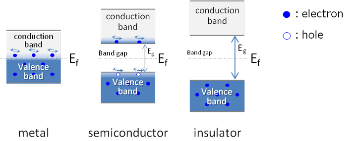
In metals, the conduction band and the valence band come very closer to each other and may even overlap, with the Fermi energy (Ef) somewhere inside. This means that the metal always has electrons that can move freely and so can always carry current. Such electrons are known as free electrons. These free electrons are responsible for current that flows through a metal.
In semiconductors and insulators, the valance band and conduction band are separated by a forbidden energy gap(Eg)of sufficient width, and the Fermi energy(Ef) is between the valence and conduction band. To get to the conduction band, the electron has to gain enough energy to jump the band gap. Once this is done, it can conduct.
In semiconductors at room temperature, the band gap is smaller, there is enough thermal energy to allow electrons to jump the gap fairly easily and make the transitions in conduction band, given the semiconductor limited conductivity. At low temperature, no electron possesses sufficient energy to occupy the conduction band and thus no movement of charge is possible. At absolute zero, semiconductors are perfect insulators, The density of electrons in conduction band at room temperature is not as high as in metals, thus cannot conduct current as good as metal. The electrical conductivity of semiconductor is not as high as metal but also not as poor as electrical insulator. That is why, this type of material is called semiconductor - means half conductor.
The band gap for insulators is large so very few electrons can jump the gap. Therefore, current does not flow easily in insulators. The difference between insulators and semiconductors is the size of the band gap energy. In insulator where forbidden gap is very large and as a result the energy required by the electron to cross over to the conduction band is practically large enough. Insulators do not conduct electricity easily. That means the electrical conductivity of insulator is very poor.
Semiconductor crystal used for IC etc. is high purity single crystal silicon of 99.999999999%, but when actually making a circuit, impurities are added to control the electrical properties. Depending on the added impurities, they become n-type and p-type semiconductors.
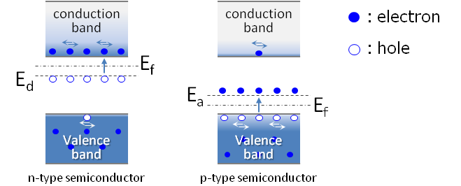
Pentavalent phosphorus (P) or arsenic (As) are added to high purity silicon for n-type semiconductors. These impurities are called donors. The energy level of the donor is located close to the conduction band, that is, the energy gap is small. Then, electrons at this energy level are easily excited to the conduction band and contribute to the conductivity.
On the other hand, trivalent boron (B) etc. is added to p type semiconductor. This is called an acceptor. The energy level of the acceptor is close to the valence band. Since there are no electrons here, electrons in the valence band are excited here. As a result, holes are formed in the valence band, which contributes to the conductivity.
Related Contents
What are semiconductors?
Semiconductor manufacturing