Semiconductor Glossary
A
ADC
ADC stands for Automatic Defect Classification. The image information of the defect stored in the image server is classified according to the cause of the defect by the classification software based on the predetermined rules and is then restored in the classification server. The classified information is sent to Yield Management System (YMS) and the host computer of the IC manufacturer so that it can be used in the failure and defect analysis. Some systems can classify defects using ADC in conjunction with the ADR function of the Defect Review SEM. The defect information obtained by ADR can also be classified collectively at a later stage.
ADR
ADR stands for Automatic Defect Review. The aim of the Defect Review is to observe, classify and analyze the shape and components of the defect and particles detected by wafer inspection system in greater detail. Automatic Defect Review automatically obtains image of the desired defect using the defect information (coordinates, etc.) obtained in defect inspection. The data is stored and arranged into a database. In Defect Review SEM, an image of the defect is automatically obtained and stored using the ADR function.
C
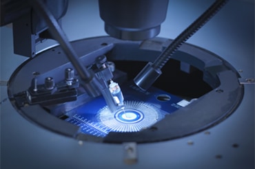
CD-SEM
CD-SEM stands for Critical Dimension-Scanning Electron Microscope. CD-SEM is application equipment for a scanning electron microscope. It is a dedicated system for measuring the dimensions of the fine patterns formed on a semiconductor wafer. It is mainly used in the manufacturing lines of electronic devices of semiconductors.
The opportunities to measure dimension of circuit pattern are mainly the following two points:
- ADI (After Development Inspection): transfer a pattern by the exposure tool, and then measure the dimension of the resist pattern after the development.
- AEI (After Etch Inspection): etch using the resist pattern as a mask, and then measure the dimensions of the etched pattern.
In case "processed pattern dimension was inappropriate", it needs to modify the processing conditions of the exposure tool (feed back).
Also at the ramp-up of a manufacturing process, it is required obtaining a relationship between the processing conditions and transferred pattern dimensions to determine the processing condition of an exposure tool by varying the conditions of the focus and the dose of the exposure tool. The FEM (Focus Exposure Matrix) is the exposed patterns onto the wafer that has been varied the conditions sequentially in this way. A process window is created using the relation of the exposure conditions (Focus, Dose) and exposure result. The optimum processing condition of the exposure tool is determined at the center of the area of the obtained process window. In this manner, CD-SEM is also used for determining the processing conditions for exposure tools.
Condenser
A condenser is a device that stores a charge in a conductor and is used as an electrical circuit component. It conducts alternating current (high-frequency) but does not conduct direct current (low-frequency) (such as accumulating electricity). In circuit design, it is used together with other components such as resistors and coils to control charging and discharging. Condenser is also used as a component in the IC.
Converter
A converter is a device used to convert alternating current (AC) to direct current (DC). It also serve as a rectifier. When using a DC electronic device from a household AC power source, AC is converted to DC by a built-in converter (AC-DC converter circuit) or by an external AC adapter. A device that converts DC to AC is called an inverter.
COP
COP stands for Crystal Originated Particle. One of the various silicon wafer surface defects. Their basic micro structure is octahedral void shape with the size of sub-micron scale.
Silicon crystals prepared using the Czochralski method and high pulling rates are grown under vacancy rich conditions, resulting in agglomeration of vacancies and formation of Crystal Originated Particles.
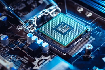
CPU
CPU, the abbreviation for Central Processing Unit, is an electronic circuit working as the core of a processing device in computers, etc.
D
Defect Review-SEM
Defect Review-SEM is the application equipment for a scanning electron microscope (SEM). The wafer defect inspection equipment detects defects on a semiconductor wafer. Then, Review SEM is used to acquire the defect's image of high magnification enough to recognize using SEM capabilities.
Die
Electronic circuit of the semiconductor device is arranged on a semiconductor wafer.
After performing various processes such as exposure and etching of the circuit patterns, die is the minimum unit of the semiconductor device to be cut out individually. Built-in to the package, by wiring the pins of the semiconductor of the contact and the IC package, IC chip is completed.
Dry etching
Dry etching is an etching method to cut the film by the force of the mechanical and chemical reaction. It excites the etching gas (chemical gas) into the plasma and etches the wafer surface by hit with the accelerated ions in the plasma. It is also able to reduce contamination and to etch highly accurately.
E
Etch system
An etch system shapes the thin film into a desired patterns using liquid chemicals, reaction gases or ion chemical reaction. It is used in manufacturing lines for semiconductors and other electronic devices.
F
FOUP (Front Opening Unified Pod)
FOUP is a closed-type wafer carrier (container) for the transport and storage, conforming to the SEMI Standard E47.1. It has an opening and closing mechanism on the front. It is commonly used in the semiconductor factory of mini-environment system of 300mm (12 inch) wafer. The inside of the FOUP keep the cleanliness of the same degree as the mini-environment system.
G
GTO (gate turn-off thyristor)
GTO is a special type of thyristor that can completely control the switch. GTO can be turned on and off by the gate signal. Conventional thyristor is not a fully controllable switch. Thyristor can only be turned on, it cannot be turned off. GTO can be turned on by the gate signal, and also, it can be turned off by the negative polarity gate signal.
GTO thyristor are usually composed of many small thyristor cells connected in parallel.
GTO thyristor has a long tail time. The tail time is the time that the residual current continues to flow after the forward current falls until all of the remaining charge from the device is taken away. GTO thyristor suffers from this long switching off time. This limits the maximum switching frequency in the audible region.
I
An electronic device comprising numerous functional elements such as transistors, resistors, condensers, etc. on a piece of silicon semiconductor substrate, and is sealed inside a package with multiple terminals.
Insulator
An insulator is a substance that does not easily conduct electricity, in contrast with a conductor that easily conducts electricity. Glass, rubber and plastics are some examples.
See also:”Properties of semiconductors”
L
Light-emitting diode
A light-emitting diode is a kind of semiconductor device that emits light when an electric current passes through it. It is also known as an LED. LEDs have a long life compared with incandescent light bulbs, and emit light using a low voltage of a few volts. Since there are LEDs in three primary colors: red, green and blue, combining them can create various colors of light.
LEDs are used in numerous areas such as household light bulbs, electric bulletin boards, traffic signals, large liquid crystal displays, etc.
M
Metrology
Metrology generally means a method of measuring numbers and volumes, mainly by using equipment (ex. CD-SEM). Metrology, though often considered synonymous with measurement, is a more comprehensive concept that refers not only to an act of measurement itself but to measurement performed by factoring in errors and accuracy, as well as the performance and mechanisms of equipment.
MEMS
N
nm (nanometer)
One nanometer is one billionth of a meter. The technology that produces the components of specific functions in nanometer dimensions is called nanotechnology in the electronic device industry. See also:“2. Metrology and inspection”
P
The Lithography, originally, means lithograph prints. Semiconductor device is made as a structure transferred onto the wafer a fine pattern by reducing exposure by using photolithography. Negative film in photo printing is the photomask (reticle: the original circuit pattern), the wafer with a photoresist (photosensitive corrosion-resistant resin coating) is corresponds to the printing paper. Photolithography is the technique for transferring a circuit pattern that is the drawn semiconductor devices on a photomask, to the photoresist on the silicon wafer using the exposure tool. It generates a pattern of the exposed portion and unexposed portions by irradiating light to the wafer through a photomask with a circuit pattern. It is called Photo-lithography because it uses a photo (light). In semiconductor manufacturing, it mainly uses the ultraviolet rays. In the semiconductor manufacturing process, it is one of the most important technologies because the formation of a fine pattern depends on it. It is also used in the manufacture of such a printed circuit board, a liquid crystal display panel and a plasma display panel. For fine pattern formation, the wavelength of light used for exposure, has been shorter and shorter. At present, sub-30nm dimension elements are able to be processed by using furrowing technologies:
- The ArF excimer laser of a 193nm wavelength
- Elaborated optical system
- Photoresist of improved sensitivity
- Immersion techniques which immersing the wafer in the water to increase the resolution,
- Multi-patterning technique which is performed plurality times of exposures in one circuit pattern formation.
In addition, the technology of extreme ultraviolet light (EUV: Extreme Ultra Violet・・・wavelength:13.5nm) is gradually being put into practical use.
Photomask
A photomask is a pattern formed on a flat plate, and is a master for transferring the different plates using photolithography technology.
Plasma
Plasma is a cloud of protons (ions), neutrons and electrons. There are solid, liquid and gas state of matter. Plasma is also one of the states of matter, the fourth state of matter. Plasma is a group of charged particles that is kept almost electrically neutral as a whole, into which sufficient energy is provided to free electrons from atoms or molecules and to allow both species; ions and electrons, to coexist. The ions with a positive charge and electrons with a negative charge are distributed equally in an ionized state.
Polycrystal
A polycrystal is made up of many minute single crystals. Each of the single crystals has its own crystal axis direction. Ceramics and many metals are polycrystals. Solar batteries are made from polycrystal silicon.
R
Random defects
Random defect is a defect due mainly to small particles generated in the semiconductor process. The random defects occurrence location will not be able to predict because the frequency of defects, the defect state and the size varies.
Resistor
Reticle
S
Semiconductor
A semiconductor is a substance possessing an electrical conductivity somewhere between that of a conductor and that of an insulator. Silicon is a representative example of a semiconductor. Its conductivity changes in accordance with the ambient temperature or the amount of impurities in them. The internal resistance falls when the temperature rises. Electronics must therefore be kept away from high temperatures. Sometimes ICs, diodes and transistors are called semiconductors, but they should be called semiconductor devices to be accurate.
Semiconductor inspection equipment (Semiconductor inspection system)
Semiconductor inspection equipment, at the semiconductor device manufacturing process, is equipment that detects the failure of the device. Semiconductor device is completed through a large number manufacturing processes. If a failure occurs during processing, the subsequent processing does not make sense. It is just to produce a defective product. Therefore, by inserting the inspection process to pivotal points of the manufacturing process, it will be advanced to the next step after confirming that there is no defect in the device. If the failure to the device is found, it interrupts the production, and then determines the cause and removes the defect. After the defect is sufficiently reduced, it is advanced to the next manufacturing step.
Equipment for detecting a defect of the device in the inspection process is the Semiconductor wafer defect inspection system. Defects in the semiconductor wafer manufacturing process are mainly small particles and pattern defects on the wafer. Semiconductor wafer defect inspection system detects physical defects (foreign substances called particles) and pattern defects on wafers and obtains the position coordinates (X, Y) of the defects. Specifying the position (coordinates) on the wafer of these particles or defects is the primary role of the inspection equipment.
Inspection can be performed on a patterned process wafer or on a bare wafer. Each of these has a different system configuration. There are many types of patterned wafer inspection systems, including the electron beam inspection systems, the bright-field inspection systems, and the dark-field inspection systems. Each of these has its own features, but the basic detection principles are the same. The non-patterned wafer inspection system is used in the wafer shipping inspection by wafer manufacturers, the wafer incoming inspection by device manufacturers and the equipment condition check using dummy bare wafers to monitor the cleanliness of equipment.
The circuit operation is tested after wafer process is completed and the electronic circuit is completed. Inspection equipment to be used in the test is also referred to as the semiconductor test equipment.
In order to maintain the production yield of the semiconductor device, these inspection equipments have become indispensable.
Semiconductor manufacturing equipment
Semiconductor manufacturing equipment is the equipment used to manufacture semiconductor devices (integrated circuits). There is a variety of semiconductor manufacturing equipment: vacuum deposition equipment for forming a thin film on a wafer, exposure tool for transferring patterns onto a wafer using the photolithography technique, etch system for forming a thin film into circuit, ion implanter for adding impurities into semiconductor, metrology and inspection equipment, assembly equipment, etc. Among the semiconductor manufacturing process, especially at the wafer processing process, small particles such as dust are the cause of the product failure. Therefore manufacturing equipment is placed in a clean room and used in a clean state.
Semiconductor metrology equipment
Metrology equipment is the equipment for measuring the various dimensions of the semiconductor circuit patterns on a wafer. CD-SEM: measure the width or diameter of the elements and patterns, ellipsometer : measure film thickness of thin film, Overlay tool for measuring a displacement of the upper circuit pattern from the lower circuit pattern.
Single crystal
In a single crystal, the direction of the crystal axis is the same in every section of the crystal. Single crystal silicon is indispensable for semiconductor manufacturing.
System LSI
Large-scale integration (LSI) is a type of IC. It is the integration of a large number of devices (transistors). The main memory of a computer is an example of this.
System LSI is a super multifunction LSI combined with single function LSIs according to the usage. It is installed inside computers and electronic devices with specific applications, such as audio devices. It makes wiring simple and helps to downsize the devices because it occupies a small area.
Systematic defects
A systematic defect occurs mainly due to the interaction of the layout and semiconductor processing.
The defect is likely to occur in combination with a particular layout pattern and a particular process.
According to the circuit pattern, the mask and the exposure process conditions, the occurring position is determined. The defects may be occurring at the same position of the circuit patterns of all of the dies that has been transferred.
The wafer defect inspection system detects defects by comparing the image of the circuit patterns of the adjacent dies. As a result, systematic defects sometimes cannot be detected using a conventional wafer defect inspection system. In such cases, it may be used a method to detect a defect by comparing the design pattern.
T
Transistor
The transistor, developed by Bell Laboratories of the USA in 1947, is a semiconductor device possessing an amplification function. It is made from germanium crystal or silicon crystal and is installed in various electronics as an alternative electron device to vacuum cube. When it is formed on a wafer together with resistors and other devices, it becomes an integrated circuit that possesses various functions.
See also: ”History of semiconductors”
Thyristor
A semiconductor device with four layers of alternating p and n-type material to perform the switching operation. It has three terminals with a gate terminal (lead) to the third p-layer of the layers. It can be interpreted as a combination of pnp and npn transistors. By passing a gate current (trigger current) from the gate terminal (control lead) to the cathode terminal of thyristor, it switches from the OFF state between the anode and cathode terminals to the ON state (conducting).
When the reverse voltage is applied to a thyristor, the current of the rectifier hardly flows. Further, when applying a forward voltage to a thyristor, it turns from the OFF state to the ON state at a certain voltage, and then the forward current flows at low voltage.
The switching voltage to an on-state would be changed by the trigger current flowing through the control terminal. As the trigger current is increased more, the switching voltage will be lower. Once having resulted in conducting, such conducting state is maintained even when the trigger current is off. It cannot be powered off by the control terminal.
There are characteristics such as small, long life, being able to control a large power with a small control power, the switching speed is high, and the structure is simple.
Thyristor is also referred to as a SCR (Silicon Controlled Rectifier).
When applied alternating current, the thyristor acts as rectifier supplying a current to each half-wave, and can change the amount of current by controlling the phase. This allows stepless control of the rotation speed of the AC motor, such as fans and washing machines.
W
Wafer
A wafer is a physical unit used for manufacturing semiconductor devices. In general, it is made by slicing a silicon ingot (a cylindrical mass) into disk-shaped pieces of about 0.5mm to 1mm thick.
Usually, silicon wafers with a 5-inch (125mm) diameter, 8-inch (200mm) diameter and 12-inch (300mm) diameter are used. There is an effort in the industry to switch to 450mkm wafers.
See also:“1. Semiconductor manufacturing process”
Wet Etching
Wet Etching is an etching method to cut film by a chemical reaction in an acid or alkaline solution to corrosion and dissolution of the film. A large number of wafers can be processed simultaneously.
Related Contents
What are semiconductors?
Semiconductor manufacturing