
Ph.D. in Engineering
Professor, Institute of Technology and Science
Tokushima University
Masao Nagase
Graphene is a remarkable carbon nanomaterial that burst onto the scene in 2004—when techniques for its isolation were first established by British researchers—and was recognized with the 2010 Nobel Prize in Physics. This material has remained the focus of intense attention to the present day1,2). Graphene boasts a wide range of mysterious and fascinating physical properties, including high mobility3) and high mechanical strength4). Its potential applications span an extremely broad range of fields. Although the easiest method for exfoliated graphene—an extremely simple fabrication technique involving graphite fragments and adhesive tape—has been widely adopted, the goal of establishing high-quality single-crystal graphene production technologies at an industrial level remains distant.
Our research group studies epitaxial graphene on SiC with the goal of achieving high-quality single-crystal graphene. In this method, single-crystal SiC is heated to high temperatures in an inert-gas environment, inducing thermal dissociation of silicon atoms from the SiC substrate to fabricate graphene5). By choosing an appropriate Si surface such as the 4H-SiC(0001) surface, one can ensure that graphene grows epitaxially on the underlying single-crystal SiC substrate, thus—in principle—yielding wafer-scale single-crystal graphene.
When graphene is transferred to a silicon substrate on which an oxide film is present, the optical properties of the resulting material may be exploited by optical microscopy to characterize the number of layers. This is one of the reasons for the intense interest in graphene research. In contrast, most studies of graphene on SiC have employed specialized techniques—such as low-energy electron microscopy (LEEM)6,7) or angle-resolved photoelectron spectroscopy (ARPEP)8)—that are relevant for only a restricted subset of researchers. However, in our experience, characterization is also possible using widely available scanning-probe microscopy. In this report, we discuss some of the results our group has achieved to date in our efforts to use various types of microscopy for characterization of graphene.
Graphene formation via silicon sublimation in an inert-gas environment requires thermal processing at temperatures of 1,600°C or higher. Although heaters based on inductive heating schemes have typically been used for this purpose, we have instead adopted infrared heating methods8), which offer outstanding controllability and uniformity. Figure 1(a) shows a photograph of our apparatus. A 2 kW infrared lamp is placed at one focus of a spheroidic mirror, while the sample is placed at the other focus. The sample is mounted on a carbon susceptor inside a quartz tube filled with inert gas (low-pressure Ar). The sample size is limited by the radius of the quartz tube to a maximum radius of 15 mm. Figure 1(b) shows a photograph of a fabricated graphene sample. We typically use a 4H-SiC(0001) substrate diced into a square with sides of 10 mm.
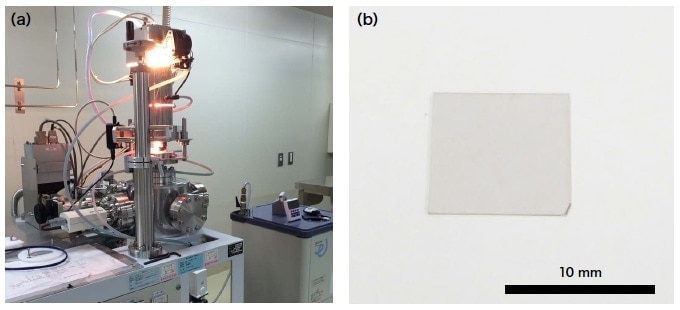
Fig.1 (a) Photograph of the ultra high-speed high-temperature infrared heating unit.
(b) A single-crystal single-layer graphene sample.
LEEM6) is known to be necessary for rigorous characterization of the number of layers of graphene on SiC samples. Microscopic Raman spectroscopy, which is widely used to characterize the number of layers of graphene samples, requires experience and meticulous caution for use in characterizing numbers of layers and film quality in graphene-on-SiC, because its spectrum differs significantly from that of oxide layers on silicon substrates9). In previous work, we have succeeded in forming uniform, single-layer graphene atop SiC substrates. Taking these samples as references, we have accumulated a body of knowledge regarding the ways in which graphene on SiC can be observed via various types of microscopy. In particular, we have empirically established a technique for using scanning-probe microscopy to characterize numbers of layers, and by evaluating the quality of the films, we make progress toward higher-quality samples. Here we present one example of a characterization of graphene on SiC using scanning-probe microscopy. The scanning-probe microscope that we use is an SPA400 (from a manufacturer currently known as Hitachi High-Tech Science and formerly known as SII Nanotechnology; we refer to this vendor below as SII-NT).
Figure 2 shows morphology images and phase images for graphene on SiC obtained via scanning-probe microscopy (SPM) observations (DFM mode) in ambient conditions. The sample is prepared by fabricating graphene on a SiC-Si face at 1,820°C in 600 torr Ar; approximately 90% of the surface is covered by single-layer graphene. In the morphology image of Figure 2(a), we see only the step-terrace structure originating from the crystal structure of the SiC substrate. In the phase image of Figure 2(b), we observe several dark regions; these correspond to regions of two-layer graphene. In this example, the regions of two-layer graphene form on terraces lying beneath step edges with step heights of 1 nm or greater [arrows in Fig. 2(a)].
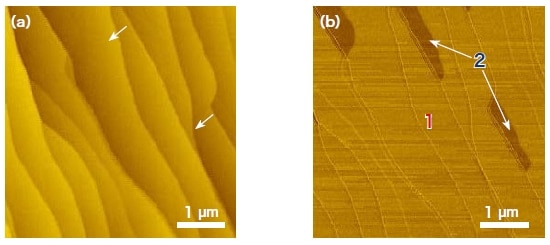
Fig.2 Scanning-probe microscopy images of graphene on SiC.
(a) Morphology image.
(b) Phase image.
Figure 3 shows the results of a more detailed investigation of these phenomena. As shown in Figure 3(a), two-layer regions are observed at a height of 0.14 nm on terraces lying beneath steps. This situation is graphically depicted in Figure 3(c).
A characteristic feature of graphene on SiC is that it grows on interfacial carbon layers (with a 6√3 × 6√3 structure) known as buffer layers; however, the growth mechanism differs from typical epitaxial growth in that the lower layers form after the upper layers. In other words, the buffer layer in the two-layer regions [Figure 3(b)] grows beneath an existing buffer layer, whereupon that portion of the original buffer layer is turned into graphene. In this example, the appearance of the two regions is clearly distinguishable in both the SPM morphology image and the phase image. Through investigations of this sort, we expand our understanding of the growth mechanisms of graphene and succeed in obtaining improvements in quality.
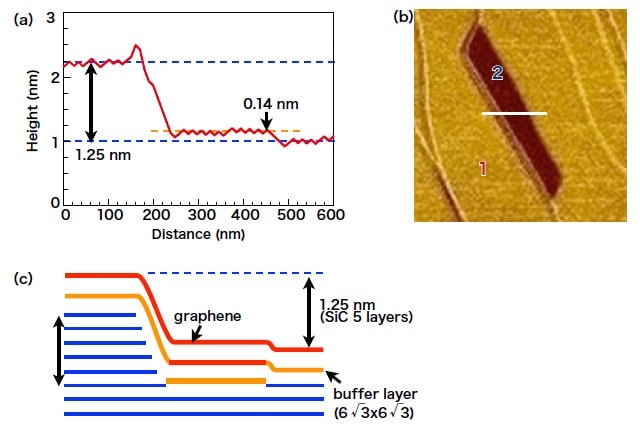
Fig.3 (a) SPM morphology profile including 2-layer regions.
(b) SPM phase image.
(c) Schematic representation of structure.
Figure 4(a) shows the surface profile of high-quality single-layer graphene obtained by optimizing fabrication conditions. As seen from the morphology image in the inset, a well-ordered step-terrace structure is obtained over the entire area of the sample (10 mm square), with a step height of 0.5 nm (SiC 2-layer regions) as shown in Figure 4(b). Because the height is fixed by the lattice constants of the SiC crystal structure, it may be used as a height reference, thus allowing calibration of the Z-sensitivity (piezo correction coefficient) of the SPM.
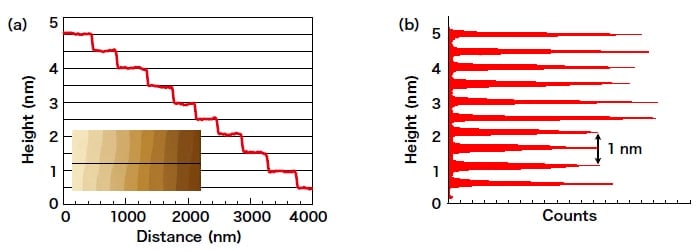
Fig.4 Single-crystal single-layer graphene surface. (a) Morphology profile. (b) Height histogram.
Graphene exhibits outstanding mechanical characteristics, and its mechanical properties include many fascinating features. Friction forces are a canonical example of a mechanical property, and one for which quantitative characterizations are of crucial importance. Figure 5 shows a sample friction-force-microscopy (FFM) image of graphene on SiC. From the friction-force image of Figure 5(b), we see that friction forces are lower in the two-layer-graphene region near the center of the figure than in the one-layer-graphene regions surrounding it. By understanding the shape of the probe tip and obtaining the dependence on loading, it is even possible to derive quantitative values for friction coefficients.
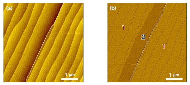
Fig.5 Friction-force microscopy images. (a) Morphology image. (b) Friction image.
For graphite, it has been known for some time that atomic-scale friction images may be obtained relatively easily. Figure 6 shows an atomic-scale friction image for graphene on SiC. The scanning direction is chosen based on the crystal alignment of the underlying SiC. It is known that the centers of the hexagonal units of the graphene honeycomb lattice (hollow sites) are imaged, and thus one obtains atomic-scale friction images, albeit not atomic images. For graphene on SiC, the crystal orientation is known in advance, and thus friction images in specific directions may be readily obtained as in Figure 6.
![Dependence of graphene friction images on the scan direction. (a) SiC[-1100] (b) SiC[11-20]](/image/global/sinews/si_report/07008/index_07.jpg)
Fig.6 Dependence of graphene friction images on the scan direction. (a) SiC[-1100] (b) SiC[11-20]
Because graphene forms across the entire surface of graphene on SiC samples, it is easy to prepare cross-sectional samples. Figure 7 shows cross-sectional transmission electron microscope (TEM) images, obtained with an H-9000, of graphene on SiC samples prepared via focused ion beam (FIB) processing. In Figure 7(a), the graphene layers, buffer layers, and SiC are observable from the black-white contrast. The problem of sample damage due to electron-beam irradiation, which is common among carbon-based materials, is also present for graphene, and for this reason the sample thickness cannot be made excessively thin; however, by predicting the graphene contrast with guidance from multi-slice simulations and repeatedly adjusting the processing parameters, we have established that effective sample thicknesses around 30 nm are optimal. Nevertheless, because sample thickness cannot be perfectly controlled, in actual samples there will be regions in which the thickness differs slightly. Figure 7(b) shows the results of TEM observations of a slightly different region (still essentially the same region) of the sample of Figure 7(a); we see that here the SiC contrast is inverted. This phenomenon is illustrated by Figure 7(c); we see that, in situations like this, it is difficult to determine the graphene–substrate interlayer distance with high accuracy. Problems of this sort do not occur when one obtains Z-contrast images using the STEM-ADF (annular dark field); however, the electron-beam radiation dose is greater for STEM than for typical TEM, whereupon the sample suffers more severe damage and high-precision measurements cannot be obtained. Interlayer distances are also important for understanding interactions between graphene and the SiC substrate and will be addressed by future work.
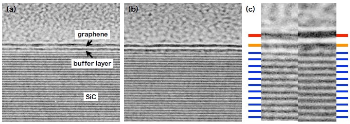
Fig.7 (a,b) Cross-sectional TEM images of graphene on SiC. (c) Comparison of (a) and (b).
In our research group, we have studied the use of focused ion beam (FIB) techniques to enrich the functionality of probes for scanning-probe microscopy. We have fabricated a variety of structures for use as integrated nanoprobes, including (a) self-detecting probe tips converted to four-point probes via FIB10), (b) four-point probes equipped with spring-attached nanocarbon probes fabricated via chemical vapor deposition11,12), and (c) two-terminal probes consisting of 30-nm-grade gap electrodes with tips subjected to FIB processing13,14). Figure 8 shows an SEM image (obtained with an S-5000 instrument) and a schematic diagram of the most basic structure: a nanocarbon probe fabricated via FIB-CVD. Here we have functionalized the probe tip of a conducting Rh-coated probe by depositing FIB-CVD carbon. For nanocarbon deposition, we use an SMI3050TB (from the former SII-NT) machine. The central core of the FIB-CVD carbon nanopillars contains significant quantities of Ga and is therefore electrically conducting. Based on the Ga beam profile, we expect that the conducting region of the nanoprobe is of size 10 nm or less.

Fig.8 SEM image and schematic representation of nanocarbon probe.
Figure 9 shows SPM morphology images and current images measured in vacuum with an E-sweep machine (from the former SII-NT). We obtain high resolution in the current image, demonstrating that the performance of our nanoprobe is adequate for our purposes.
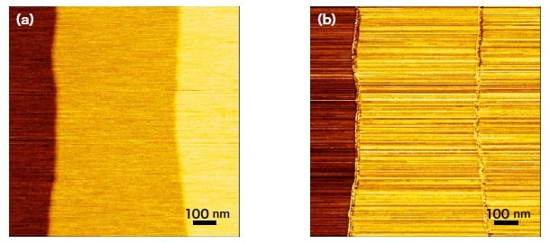
Fig.9 SPM images obtained with nanocarbon probe. (a) Morphology image. (b) Current image.
We have presented a selection of results of observations of graphene on SiC, obtained primarily by scanning-probe microscopy. Compared to exfoliated graphene, graphene on SiC exhibits lower mobility and other disadvantages and is generally believed to be of inferior quality. On the other hand, it is an excellent technique for obtaining single-crystal graphene at wafer scales. Improving the quality of graphene on SiC will require quantitative characterization using a variety of characterization methods. At present, efforts to optimize fabrication parameters generally rely primarily on microscopic Raman spectroscopy and various other similar types of microscopy. To date, these efforts have reached the point of obtaining films of quality generally equivalent to that of exfoliated graphene15). We plan to solve a variety of further problems in the service of obtaining even higher quality.
Because graphene on SiC yields uniform samples of relatively large areas, they are well-suited as samples for various types of microscopy. Moreover, because the physical properties of graphene on SiC samples are stable, they may be used as standard reference samples for various material properties. In particular, they may be used as standards for gaps, as demonstrated in this report. Furthermore, because their surface morphology is stable, they may also be used as standard reference samples not only for friction coefficients and a variety of other mechanical properties but also for surface potentials and measurements of electrical current (contact properties)16,17).
References
Acknowledgements
Portions of this research were conducted with support from JSPS research grants (Grant Numbers 26289107 and 22310086) as well as A-STEP FS Search support (AS231Z00351B). Some results reported in this paper were obtained in collaboration with NTT Basic Research Laboratories.
See more
