
Daisuke Fujita
Executive Vice President
National Institute for Materials Science
Fine-grain control of the structure of materials is widely regarded as a crucial technology undergirding innovation in materials science. Today, thanks to nanotechnology initiatives launched at the beginning of the 21st century, materials and device elements with a fi ne grain structure can be produced and distributed as nano-products. According to the International Technology Roadmap for Semiconductors (ITRS), prototype development for LSI chips with 10-nm gate lengths is already underway, and single-digit nanoscale elements are expected to become a reality within the next few years. The number of dopant atoms that can be present in the channel of this sort of nanosized transistor is on the order of 1. Developments like these dictate that, by necessity, cutting-edge nanoscale measurement technologies with single-atom resolution will become standard, and will be essential for innovation to occur. Measurement technologies that allow single-atom analysis in real space include transmission electron microscopy (TEM) and scanning probe microscopy (SPM).
In 2001, Fujita et al. proposed combining environmental conditions, known as "active manipulation" to yield a nextgeneration nanoscale measurement technique for materials research.1) In this paradigm, the environmental conditions in which a material was fabricated, or in which it expresses the desired functionality, are replicated in order to analyze the mechanisms of functional expression and the material fabrication process at the nanoscale. In recent years, this paradigm has been complemented by an emphasis on operando measurements conducted on a material or device in its actual operating state. The word "operando" is derived from the Latin for working. The notion of operando observations was proposed around the year 2002 in the field of catalysis research, where operando spectroscopy was presented as "a methodology that combines the spectroscopic characterization of a catalytic material during reaction with the simultaneous measurement of catalytic activity/selectivity".2) Today, the term is no longer restricted to the field of catalysis research. Any direct measurement or observation in the actual operating environment of a device or material, designed to elicit certain desired functionality, may be called an operando measurement or observation. In particular, SPM techniques are ideally suited to operando nanoscale measurements for atomic level analysis of nanostructure fabrication and functional expression at material surfaces and interfaces.
In SPM techniques, a probe with a sharp tip is scanned over a material surface to measure physical properties and functionality at the nanoscale. Common varieties of SPM with atomic resolution include scanning tunneling microscopy (STM) and atomic force microscopy (AFM). In STM, the tunneling current between the tip and sample surface is used as a control signal to allow non-contact measurements with the spatial position controlled with a precision on the order of picometers. Since the emergence of STM, which was invented in 1982, it has become a tool not only for visualizing but also manipulating individual atoms in real space. This revolutionary advance was recognized by the awarding of the 1986 Nobel Prize in Physics to Binnig and Rohrer, the inventors of STM. Although STM requires the sample surface to be electrically conducting, AFM – which may be used to observe insulators – was subsequently invented by Binnig, Quate, and others in 1986. In AFM, the interaction force between the tip and sample surface is used as a control signal to allow visualization of structures at the nanoscale. This method may be used to observe a wide range of nanomaterials, including insulators and materials containing biomolecules.
SPM allows the functions and physical properties of materials to be measured at the nanoscale. Many specialized analysis modes have been developed, allowing investigation of not only the morphology and atomic structure, but also mechanical properties, electrical properties, magnetic properties, and various other nanoscale physical properties. Many of the functions exhibited by nanomaterials arise from quantum effects, requiring an understanding of novel electronic states arising due to closed nanoscale structures or reduced dimensionality. STM is the most powerful spectroscopic visualization method for electronic states. Scanning tunneling spectroscopy (STS) allows visualization of the local density of states (LDOS) at surfaces. To identify the LDOS at various energies near the Fermi level, the differential tunneling conductance (dI/dV) is measured. The tunneling current I can then be expressed as the convolution of the tip profile with the sample LDOS. If the variation in the LDOS at the tip is gentle, the quantity dI/dV near zero bias is proportional to the surface LDOS. dI/dV images are obtained by superposing a modulating (frequency-ω) sine wave a top the bias, and then using a lock-in a mplifier to measure and plot the modulated (frequency-ω) component of the tunneling current. Applying a two-dimensional fast Fourier transform (FFT) to the LDOS image allows visualization of physical properties in k-space, such as the reciprocal lattice, the lowerdimensional Fermi surface, and the band structure.
The use of STM/STS allows electronic states in the vicinity of a single dopant atom to be visualized at various energies (Figure 1). As the miniaturization of semiconductor devices such as CMOS FETs proceeds, the ability to obtain detailed information on electronic states (including band bending) in the vicinity of single dopant atoms in conducting channels will yield important insights for electronic device development. Similarly, the use of spinpolarized electrons in STS allows surface magnetic properties to be analyzed with atomic resolution, aiding the development of spintronic devices and nanomagnetic materials. To develop these techniques further as tools for studying physical properties and function will require working conditions in which quantum effects are clearly discernible, including ultra-low temperatures, high magnetic fields, and ultra-high vacuums, pushing environmental control requirements to extreme limits.
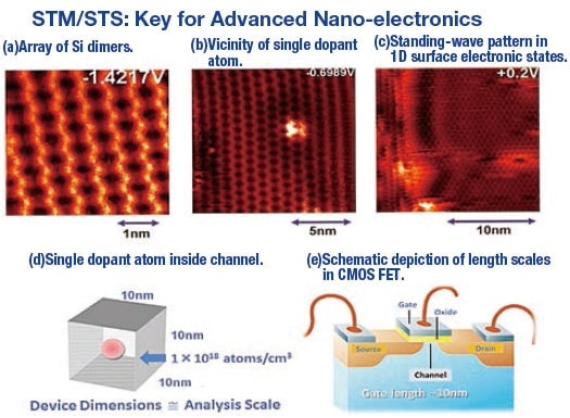
Fig.1
Nanoscale imaging of Si(001) surface using ultra-low-temperature STM/STS.
SPM not only makes possible a rich selection of atomic scale measurements, but can also be used to perform a variety of nanofabrication tasks, including manipulation of single atoms. The wide range of measurable physical quantities that can be observed via SPM methods – which includes the density of states, near-field light, spin polarization, inelastic tunneling spectroscopy, the local work function, electric potentials, and magnetic and mechanical properties – testifi es to the broad usefulness of SPM techniques. Examples of the extensive variety of ways in which SPM can be used for nanofabrication include single-atom manipulation, nanoscale molding and forming, selective local oxidation, nanolithography, and tip mass transport. Thus, SPM methods offer extremely powerful capabilities for both nanoscale fabrication and many types of high-resolution measurements in actual operating environments.
SPM nanoscale measurement techniques, the foundation on which nanotechnology is built, can be divided into two categories (Figure 2). The first class of methods combines nanofabrication and nanoscale measurements into a paradigm inspired by the notion that Scanning is creating. In this approach, stress, temperature, pressure, vacuum level, radiation, and other environmental conditions are tightly interwoven with the material fabrication process. A second class of methods consists of multifaceted operando nanoscale measurements, performed within the functional expression environment, with the goal of elucidating the mechanisms of functional expression – a strategy we might term the Seeing is discovering approach. Many nanomaterial functions arise from quantum effects that emerge prominently under circumstances that are extreme in multiple ways: ultra-low temperatures, high magnetic fields, ultra-high vacuums, or similar environments. Ultra-low temperatures suppress thermal fluctuations, allowing the observation of quantum effects involving electrons. Phenomena that may be observed under such conditions include interference among low-dimensional electron waves, single-electron effects, and inelastic tunneling. Strong magnetic fields play an important role in studies on spin effects, superconductivity, Landau quantization, and other similar phenomena. Thus, SPM operando nanoscale measurement is a technique for analyzing surface behavior in "living" samples.
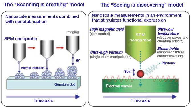
Fig.2
Principles of surface SPM operando nanoscale measurement techniques.
Within the nanotechnology sector, strategies for meeting the dual needs of nanofabrication and direct characterization are essential. These include the fusion of nanofabrication and in-situ nanoscale measurements: nanostructure fabrication by tip induction, control of surface structure via control of injected electron energy, singleatom manipulation, fabrication of low-dimensional quantum nanostructures, and manipulation of nanoclusters. An important breakthrough demonstrating the achievement of atomic-level manipulation was the world's first successful reversible manipulation of one-dimensional periodic structures on a Si(100) surface – a staple semiconductor material – by controlling the energy of carriers injected from a probe tip (Figure 3).3) By controlling the potential difference between the probe and the sample surface.thus controlling the energy of electrons or holes injected into the surface.we successfully achieved reversible phase manipulation, converting the surface from a c(4×2) structure (the ground state of the Si(001) surface) to a metastable p(2×2) structure (Figure 4).
Moreover, by combining this idea with a method for transferring individual atoms from a probe tip to a surface, we developed a technique for inducing a closing off – within a nanoscale region – of the one-dimensional surface electronic states formed by an array of Si dimers, due to the potential barrier created by the transferred atom. For this experiment, we fabricated a one-dimensional quantum well structure based on a Si dimer array at an atomic level, and developed a LDOS imaging technique to visualize the quantized energy levels inside the quantum well.4)
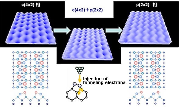
Fig.3
Discovery and manipulation of periodic structure on Si(100) surface using ultra-lowtemperature, ultra-high vacuum STM. Superstructure control is achieved by controlling the energy of electrons or holes injected into the dimer.
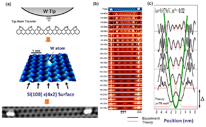
Fig.4
(a)Using ultra-low-temperature STM to transfer W atoms from a probe tip to a Si(100) surface dimer and fabricate surface states with closed structures
(b)Using STS to visualize LDOS in a one-dimensional quantum well
(c)One-dimensional harmonic oscillator model showing agreement with data
The environmental conditions that are important for materials research include temperature, needed to characterize properties such as the thermal resistance of materials; the gas atmosphere, needed to characterize catalytic materials and other substances; stress, needed to control physical properties by inducing lattice distortion; and inert-gas environments, needed to characterize materials for batteries. The development of SPM measurement techniques with environmental control related to innovations in materials is already underway. Examples include (a) atomic-resolution SPM methods in high-temperature gas environments, and (b) atomic-resolution SPM methods under externally controlled stress fields.
The stability of ultra-thin oxide layers on semiconductor surfaces is important for industrial applications, and phenomena such as high-temperature decomposition of SiO2 thin films have been studied using methods such as low-energy electron microscopy (LEEM). Although STM is a powerful tool for atomic-resolution observations at high temperatures and under ultra-high vacuums, the fact that SiO2 thin films are electrically insulating makes STM difficult to apply to films with thicknesses of greater than 2 nm. On the other hand, high-temperature noncontact AFM (NCAFM) measurements of insulating surfaces using standard cantilever tips suffer from the difficulty that, because the surface and the sensor lever are in close proximity, thermal radiation effects become prominent, preventing this approach from offering adequate performance. However, a crystal-oscillator force sensor with a highmelting-point metallic tip (a needle sensor) maintains a greater distance from the surface than a cantilever-type probe, which should reduce thermal radiation effects for force sensors and allow operation at high temperatures. We built a temperature-tunable ultra-high-vacuum SPM system that uses a crystal-oscillator probe and is capable of measuring both NCAFM and tunneling currents, and using this instrument we successfully observed the high-temperature decomposition of an ultra-thin SiO2 film.5) In NCAFM height images and tunneling-current images of an SiO2/Si(111) surface maintained at a temperature of 950 K, we observed the formation of electrically conducting voids and the growth of nanoprotrusions at the void centers. In STM mode we observed that the interiors of the voids had a Si(111) 7×7 surface reconstruction. Whereas previous models considered only the reductive desorption reaction at the oxide film, our findings demonstrated that the process is a more complex phenomenon involving competition among three effects: (1) the reductive desorption of SiO(g), (2) the formation of nanoprotrusions due to re-binding of mobile Si atoms created within the voids, and (3) layer-by-layer etching.
We developed a temperature-tunable, ultra-high-vacuum NCAFM/STM system with atomic resolution and an externally-controlled stress field (Figure 6), and used this instrument to investigate the reorganization and structural variation of a Si(001) surface due to stress-induced distortion.6) Stress is an increasingly important control parameter in the field of semiconductor research, with applications including band engineering and improved carrier mobility, and high-precision SPM nanoscale measurements offering control over lattice distortion have been eagerly anticipated.
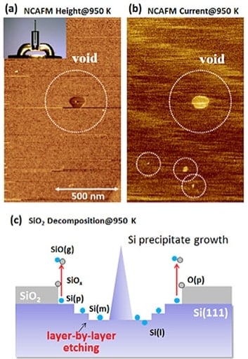
Fig.5
Simultaneously captured (a) morphology image, (b) tunneling-current image of an ultra-thin SiO2 film obtained via needle-sensor NCAFM at high temperature and under high vacuum. (c) Model of void growth and nucleation of Si protrusion.
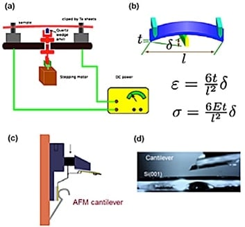
Fig.6
Development of SPM in stress fields.
(a) Application of uniaxial stress.
(b) Quantifying stress and distortion.
(c) Schematic diagram of scanning-tip AFM mechanism.
(d) NCAFM measurement in the presence of applied stress.
Spurred in part by growing interest in environmental energy problems, materials and devices for energy conversion, such as photovoltaic cells (PVCs), and energy storage, such as lithium-ion batteries, have become a focus of intensive research effort. Further improvements in device performance will require a deeper understanding of the principles governing device operation–an objective for which it is essential to be able to measure and characterize the physical properties of devices, and their variations, directly while the device is in operation.
In PVCs, which convert optical energy into electrical energy, measurements of quantities such as the potential near excitation centers under irradiation or in the presence of applied voltages, electronic states, and charge distributions can yield valuable insights into the optical-electrical conversion process (Figure 7). Thus, the notion of operando measurements–in which the physical properties of a device are directly characterized while the device is in operation.has become a focus of attention. However, these measurements have been mainly performed by researchers in the field of electronic spectroscopy or X-ray spectroscopy, and such techniques do not offer sufficient spatial resolution for the characterization of next-generation devices, which make heavy use of nanostructures. For these reasons, as operando measurements that can characterize local properties at the nanoscale or the atomic scale, we are developing core technologies (including cross-sectional SPM and SPM in optical irradiation fi elds) for STM/STS (useful for structures or electronic states) and for Kelvin-probe force microscopy (KPFM) that can operate in a wide variety of environments including optical irradiation fi elds, in the presence of applied voltages, in inert-gas environments, and in ultra-high vacuums (Figure 8).
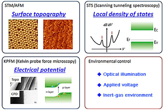
Fig.7
Using operando SPM to measure a PVC during actual operation.
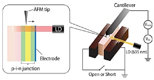
Fig.8
Development of cross-sectional SPM in optical irradiation field: Operando nanoscale measurement of PVC surface under irradiation by visual light
KPFM–a characterization method capable of nanoscale measurement of surface potential distributions–has been applied in recent years to the characterization of a wide variety of devices. In KPFM, the electrostatic force acting between the tip and sample is used to measure the contact potential difference (CPD) (Figure 9). Because electrostatic forces are long range, the CPD obtained at a given point represents an average over a relatively wide area of the sample surface (the probe averaging effect). This effect not only results in reduced spatial resolution, but also complicates quantitative characterization of the potential. Moreover, this effect is particularly pronounced in the commonly used amplitude-modulation version of the technique (AM-KPFM). We investigated the impact of the probe shape on the averaging effect, and used an electrode pattern for which the potential was known in order to characterize the distance dependence of the averaging effect. After data correction based on this observed distance dependence, we were able to obtain quantitative agreement between potential measurements using operando KPFM and the open-circuit voltage for a PVC.
The highly innovative fi eld of secondary batteries–devices expected to play key roles in addressing problems in the energy sector–requires operando nanoscale measurements of ion migration and variations in electric potential. For example, research on lithium-ion batteries (LIBs) demands techniques for nanoscale visualization of lithium ions during the charge/discharge process, and techniques based on scanning Auger microscopy and other approaches have been developed.7,8) All-solid-state LIBs have been proposed as safe next-generation secondary batteries that combine high capacity and high density. Solid electrolytes offer the advantages of being safe and non-combustible, and materials whose ionic conductivity rivals that of liquid electrolytes are currently under development. However, the devices exhibit problems relating to interfacial resistance and non-optimal performance. For all-solid-state LIBs, improving the device performance requires an understanding of not just the Li distribution and the morphology, but also the potential distribution during device operation, a task requiring operando techniques for potential measurements. To measure the potential distribution inside an all-solid-state LIB while the battery is operating, we have developed core technologies in which the LIB is charged and discharged in an inert-gas environment while cross-sectional potential nanoscale measurements are performed using a glove-box KPFM (Figure 10).
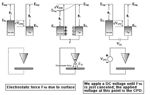
Fig.9
Principles of KPFM measurements.
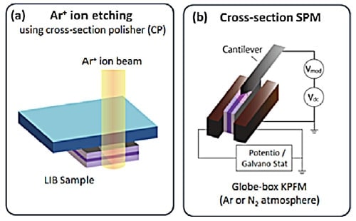
Fig.10
(a) Cross-sectional polishing of all-solid-state LIB.
(b) Operando potential nanoscale measurements using glove-box KPFM.
In this article, we have discussed some current trends in SPM-based operando nanoscale measurements. Because demand for such measurements arises from a wide range of industrial applications, in the future it will be necessary to evolve these techniques into standardized measurement methodologies. We will also need innovations to identify novel operando nanoscale measurement techniques, which are currently at the embryonic stage of laboratory-level development, and grow these into mature methods applicable to real-world systems. These sorts of innovative new measurement paradigms require basic research to quantify their performance and other benchmarks. To disseminate and standardize new methods also requires initiatives conducted within a framework of international collaboration. For standardization efforts in the SPM field, the theatre of activity is SC9 (SPM), established by provision TC201 (Surface Chemical Analysis) of the International Organization for Standardization (ISO).9) In the past we have played the role of coordinating international deliberative bodies for ISO/TC201 and TC202 (Micro-Beam Analysis). In the future, as the standardization of operando SPM measurement proceeds, researchers affiliated with Japan’s national laboratories. including the National Institute for Materials Science (NIMS) and the National Institute of Advanced Industrial Science and Technology (AIST).are expected to play leading roles.
References
See more
