Satoshi Hasumura*1
The AFM5000II scanning probe microscope station handles control and imaging for scanning probe microscopes capable of observing morphologies and analyzing physical properties in the nanoscale regime. It is designed to allow easy operation for experimentalists of all experience levels. In this short note, we review the operating principles and configuration of scanning probe microscopes, and then discuss the features incorporated into the AFM5000II for the automatic adjustment of measurement parameters to improve the ease of operation.
Scanning probe microscopes are instruments that measure a variety of physical quantities, including forces, hardness, elasticity, friction, electric currents, and magnetic interactions, using the interaction between the atoms in a sample and a probe tip. They allow for morphological observations and the mapping of physical properties for sample surfaces at the nanoscale.
Figure 1 shows the configuration of a scanning probe microscope. When a cantilever equipped with a sharp tip—whose radius of curvature is on the order of nanometers—is brought into close proximity with a sample, physical forces acting between the tip and the sample give rise to a deflection of the cantilever. The cantilever deflection is detected using optical lever methods, which involve a semiconductor laser and a light sensor. The physical forces between the tip and sample vary depending on the surface characteristics of the sample, and when a microactuator is used to scan the tip across the sample in the in-plane (XY) direction, the cantilever deflection varies accordingly. For forces that depend on the tip-sample distance, the cantilever deflection reflects information regarding the surface morphology of the sample.
The most commonly adopted approach is to use a microactuator in the vertical (Z) direction to drive the cantilever near its characteristic resonance frequency to ensure that its deflection (the amplitude of its vibrations) remains constant. By displaying the control signal applied to this vertical actuator as the probe is scanned in the in-plane (XY) direction, the three-dimensional morphology of the sample surface is obtained.
As shown in Figure 1, the AFM5000II comprises an electronic circuitry unit and a CPU (which includes software for probe microscopy).
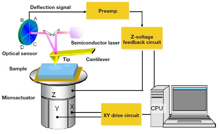
Fig.1 Configuration of scanning probe microscope.
Figure 2 shows photographs of the AFM5000II. The station, including all of the electronic circuitry, occupies roughly as much space as a desktop PC, offering users freedom in choosing an installation location. As shown in Figure 2, the AFM5000II may be combined with various units (such as the AFM5100N or AFM5300E) to construct a scanning probe microscopy system.
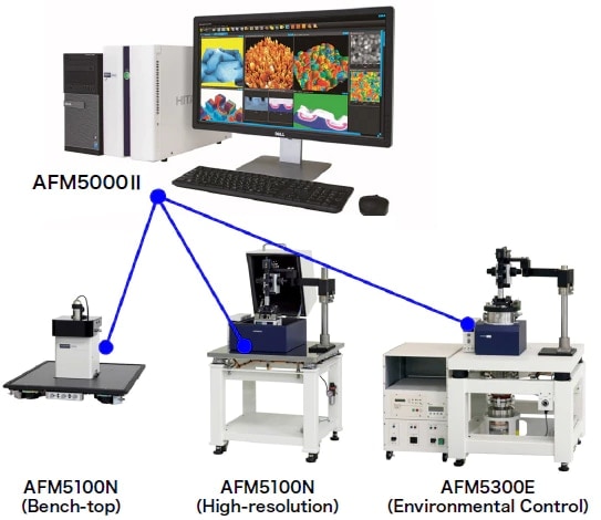
Fig.2 Photographs of the AFM5000II.
Scanning probe microscopes allow for the mapping of not only surface morphologies but also various physical quantities such as electrical or magnetic forces. For this reason, they are used in a wide range of applications across many fields of research, including organic and polymer materials, electronics, and the biosciences. The types of samples that can be measured range from hard, flat surfaces, such as wafers, to soft structures possessing some degree of roughness, such as functional materials, polymers, and biological organisms, and even to powdered materials.
For accurate imaging, the probe tip must accurately track the sample surface throughout the measurement. This requires that users adjust a large number of measurement parameters to determine the optimal measurement conditions based on the properties of a given sample. For example, when making measurements of samples with significant roughness, an appropriate value for the feedback gain must be chosen to ensure that the tip does not recede from the sample surface during the retraction phase. Similarly, depending on the spatial frequency of the sample surface morphology, it may be necessary to reduce the XY scan speed.
However, when attempting to select the optimal values of measurement parameters for a sample of unknown morphology, failure to identify the proper settings can cause problems. Moreover, some pairs of parameters are coupled, so it is difficult to obtain accurate measurements with a scanning probe microscope unless one is a fairly experienced operator.
To address these issues, the AFM5000II is equipped with new functionality we have developed for automatically determining the appropriate settings for a large number of measurement parameters. More specifically, the sample is scanned for a brief period of time to gather control error signals and other types of information. Then, based on this information, optimal values are computed for parameters such as feedback gain, scan speed, force control during the measurement, and cantilever vibration amplitude.
Figure 3 shows an example of a measurement made using the AFM5000II. The polycrystalline pentacene film portion of an organic thin-film transistor is a sample whose surface is easily destroyed; nonetheless, we see that the automated adjustment of the measurement parameters allows stable measurements of the molecular step structure.
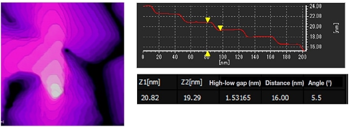
Fig.3 Polycrystalline pentacene film of an organic thin-film transistor. (Sample provided by the Kitamura Laboratory, Kobe University.)
Figure 4 shows the results of measurements of a fibrous carbon nanotube structure. This sample, which is both soft and possesses a rough surface, requires fine adjustment of the measurement parameters. When the tip makes excessively strong contact with the sample surface, the soft fibers deform (left image in Figure 4). On the other hand, when the contact force is too weak, the tip does not penetrate into the gaps between the fibers, and an accurate image of the surface morphology is not obtained. Through the use of the AFM5000II's automated parameter optimization, we obtain accurate images without damaging the sample (right image in Figure 4).
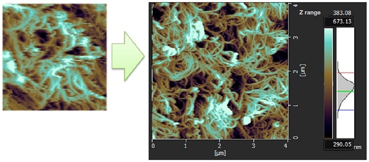
Fig.4 Fibrous carbon nanotube structure (Gecko tape). (Sample provided by Nitto Denko.)
In addition to the automatic parameter adjustment functionality discussed above, the AFM5000II features an attractive, simple, and intuitive graphical user interface. This allows even novice experimentalists to obtain accurate and reproducible images of samples, even when imaging the sample for the first time. The instrument even offers a one-click measurement mode, elevating the ease of use to an entirely new level.
Today, scanning probe microscopes are used not only for research and development but also for quality control and on manufacturing lines. The expansion of applications such as these brings increasingly urgent calls for instruments that can be operated by essentially anyone—a need we can say with confidence to have satisfied by developing and offering the AFM5000II.
Author
*1Satoshi Hasumura
Analytical Instruments Design Department,
Engineering Division,
Hitachi High-Tech Science Corporation
See more
