Nanoscale Device Characteristics Analysis System Nano-Prober NP8000
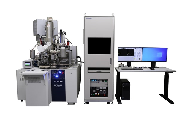
The Hitachi NP8000 is a SEM-based dedicated probing system designed to meet the analytical needs of 5 nm nodes and beyond. The system is capable of evaluating electrical characteristics, EBAC, EBIC, pulse IV, and the temperature requirements of nanoscale devices.
Overview
- New electron optics and new Schottky electron gun enable clear imaging using ultralow acceleration voltages of less than 100 V
- Improvement of EBAC image quality with high probe current
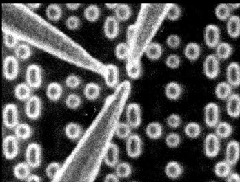
- 8 probe compatible
- Temperature-controlled stage for temperature-dependent characterization
- OM camera for both top-down and side views to assist coarse probing
- Sub-stage to allow samples to move independently from probes
- Probe exchange load-lock chamber
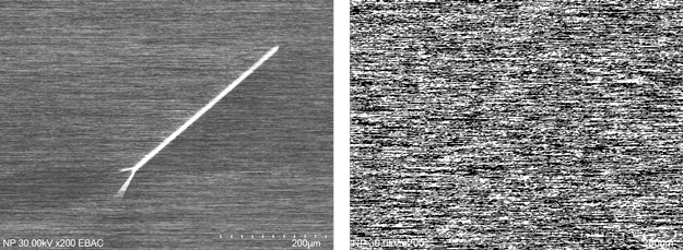
- EBAC (Electron Beam Absorbed Current) imaging function
- Improved voltage-applied EBAC function (dynamic-induced EBAC "DI-EBAC")
- Pulsed IV measurement for diagnosing resistive gate electronode defects (custom order)
Features
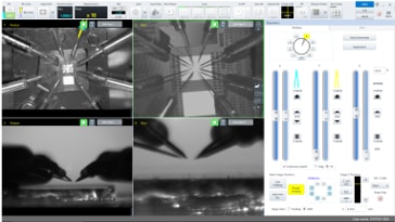
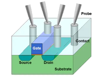
Integrated GUI for probe-position control and SEM imaging
Simultaneous display (top and side) ensures accurate positioning
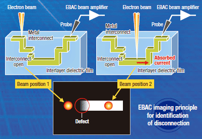
Simultaneous display of SEM and EBAC images
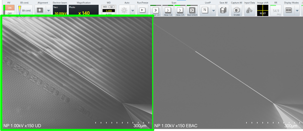
A method for faster defect detection
Low-resistance defects have historically been hard to image. The NP8000 is equiped with a new Schottky electron gun and improved voltage-applied EBAC amplifier that allows for easy imaging of these defects.
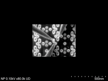
Improved imaging capability at low-accelerating voltages allows for lower accelerating voltages to be used which reduces specimen damage during observation.
Accelerating voltage: 100 V
Magnification: 80,000 (Live image)
Specifications
| Probe unit | Number of Probes | 8 |
|---|---|---|
| Stage Type | Piezoelectric | |
| Fine stroke range | 5 µm (X,Y) | |
| Coarse stroke range | 3 mm (X), 5 mm (Y) | |
| Specimen stage / Base stage |
Specimen size | 15 mm x 15 mm or smaller (1 mm thick or less) |
| Travel Range | Measurement / Specimen exchange / Probe exchange | |
| Specimen / probe exchange |
Air-lock exchange chamber equipped | |
| Probe navigation | Stage traverse to probe position Measurement position memory |
|
| Probe coarse adjustment | ||
| Probe coarse adjustment | OM image display | Top-down and side image displays |
| Electron optics | Electron gun | Schottky emission electron source |
| Accelerating voltage | 0.1 kV to 30 kV | |
| Image shift | ±75 µm (at Vacc=1.0 kV, WD=5 mm) | |
| EBAC amplifier / Image display |
Amplifier type | Current amplifier / Differential amplifier/DI-EBAC amplifier |
| Image display | SEM / EBAC (Single / Parallel / Overlay) | |
| Image processing | Black and white reversal display, color display, brightness adjustment, slow scan integration, belt scan |
This journal addresses a wide range variety of research papers and useful application data using Hitachi science instruments.
Related Information

Hitachi High-Tech Social Media