
Advanced CD Measurement SEM CS4800
A sustainable CD measurement solution to a wide range of 4, 6, and 8 inch wafer Fabs
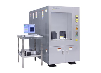
The Advanced CD Measurement SEM CS4800 provides high-quality SEM imaging, improved measurement precision, and fast, automated operation, designed to improve productivity and operating efficiency of existing manufacturing lines and increase customer's process control capability. In addition, the CD-SEM: CS4800 can be configured to handle two different wafer sizes that can be switched by the customer using to a new wafer-transfer system. Various wafer materials such as Silicon Carbide (SiC) and Gallium Nitride (GaN) to meet diversified customer's needs for new semiconductor or electronic devices are supported.
Features
- Tool footprint and GUI*1 are designed for easy replacement of existing tools.
- Proven high-precision measurements, latest metrology applications are available.
- Automated optics axis alignment will reduce operator errors.
- High throughput, automated recipe measurement operation with robust pattern matching.
- Multiple wafer size option available.
*1 GUI (Graphic User Interface): A software operating system interfacing a computer's graphic display with the use of a mouse and other pointing devices.
Specifications
| Measurement Precision | 1 nm (3σ) (Using Hitachi Standard Wafer) |
|---|---|
| Wafer size | 100, 150, and 200 millimeters in diameter |
| Auto-loader | 2 ports |
| Equipment size (main body) in millimeters | 1180(W) × 2500(D) × 1990(H)mm |