


Field Emission SEM for High-Resolution Materials and Battery Imaging
Provided by Environmental Business Division | Published: November 17, 2026
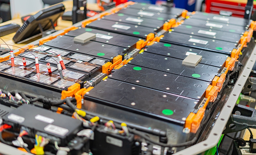
Battery cells, ore samples, and engineered parts all hide their most important features at the nanoscale. A tiny crack in a cathode particle can shorten cycle life. A thin rim on a mineral grain can change how it behaves during processing. A field emission SEM gives researchers the resolution and surface detail needed to see these features clearly.
That capability now sits at the center of modern materials characterization. Battery developers, geologists, and process engineers rely on it to connect structure with performance. The sections below explain how the technology works and where it delivers the most value.
How a Field Emission SEM Achieves Higher Resolution
A field emission SEM pulls electrons from a very sharp emitter tip using a strong electric field. This source is far brighter than a conventional tungsten filament, and it produces a narrower energy spread. Together, these traits create a smaller, more-focused probe on the sample.
A smaller probe reveals finer detail. Modern field emission scanning electron microscopes can resolve features below one nanometer. They also hold strong image quality at low accelerating voltages. That low-voltage performance brings several practical benefits:
- Sharper surface detail, since low-energy electrons probe a shallower region of the sample.
- Less charging on insulators such as separators, binders, and silicate minerals.
- Reduced beam damage on polymers and other sensitive phases.
- Stable probe current for long EDS-mapping runs, especially with Schottky sources.
Two main-source designs are common. Cold field emission offers very high brightness and a narrow energy spread. Schottky emission delivers high, steady beam current for analytical work. Both outperform thermionic sources at high magnification.
Imaging Battery Materials with a Field Emission SEM
Battery performance depends heavily on microstructure. Small defects in electrodes and separators can explain capacity fade or safety issues. A field emission SEM helps teams find these features early in development. Typical imaging targets include:
- Cathode particles, where researchers check for cracking, grain boundaries, and coating uniformity.
- Anode materials, including graphite morphology, silicon expansion, and lithium plating.
- Separators, where fiber width, pore size, and surface roughness affect ion transport.
- Binder and conductive carbon networks that hold the electrode together.
Many of these materials are delicate. Polymer separators can charge or deform under a high-energy beam. Low-kV imaging often lets analysts view them without a conductive coating. That keeps the true surface visible.
Air exposure is another challenge. Charged anodes and lithium metal react quickly with oxygen and moisture, and even brief exposure can alter the surface under study. Many labs keep these samples isolated from preparation through imaging, using tools such as the Air Protection Holder Unit on the IM4000II Ion Milling System.
Pairing images with EDS mapping adds chemical context. Teams can then link particle structure to composition and cell performance.
Preparing Clean Cross Sections for Battery and Mineral Samples
Great images start with great samples. Mechanical polishing can smear soft layers, pull out particles, or leave scratches, and these artifacts hide the true structure of electrodes and mineral grains.
Broad argon ion milling offers a cleaner alternative. The ion beam gradually removes material across a wide area, leaving a flat surface with minimal mechanical damage that is ready for high-resolution imaging and EDS.
This approach suits multilayer battery electrodes well because it preserves the interfaces between the current collector, active material, and coatings. Cryogenic cooling helps protect heat-sensitive polymers and binders.
Mining and geology samples benefit too. Ion-polished surfaces reveal fine grain boundaries, inclusions, and alteration rims. Flat surfaces also improve EDS accuracy and EBSD pattern quality. That precision supports reliable mineral identification and better process decisions.
Field Emission SEM Solutions from Hitachi High-Tech
Hitachi High-Tech offers several platforms that support these workflows. The SU3800SE and SU3900SE are high-resolution Schottky FE-SEMs with 0.9 nm secondary-electron resolution at 30 kV. The SU3900SE accepts samples up to 300 mm in diameter and 130 mm in height, and its Auto Alignment Sequence helps users of all skill levels capture consistent images.
For multi-signal research, the SU7000 can process, display, and save up to six signals at once. Its chamber accepts specimens up to 200 mm in diameter and offers 18 accessory ports for complex battery and materials work.
The FlexSEM 1000 II brings variable-pressure imaging to a compact footprint, which suits routine screening and quality control close to production.
Mining and battery recycling teams can add AMICS automated mineralogy software. AMICS pairs large-area mapping with smart EDS point placement to classify phases automatically. It runs on a variety of Hitachi SEM and FE-SEM systems and can assist in classifying difficult phases.
Application specialists work closely with each lab to match instruments to real workflows, and responsive service helps keep systems productive for years.
Take the Next Step Toward Sharper Materials Insight
Every lab works with its own mix of materials, throughput goals, and space limits. Our team can review your samples and help you compare imaging and preparation options. Contact our team to find the field emission SEM that fits your battery, mining, or materials research.