


Materials Characterization for Semiconductor R&D Beyond Failure Analysis
Provided by Environmental Business Division | Published: November 20, 2026
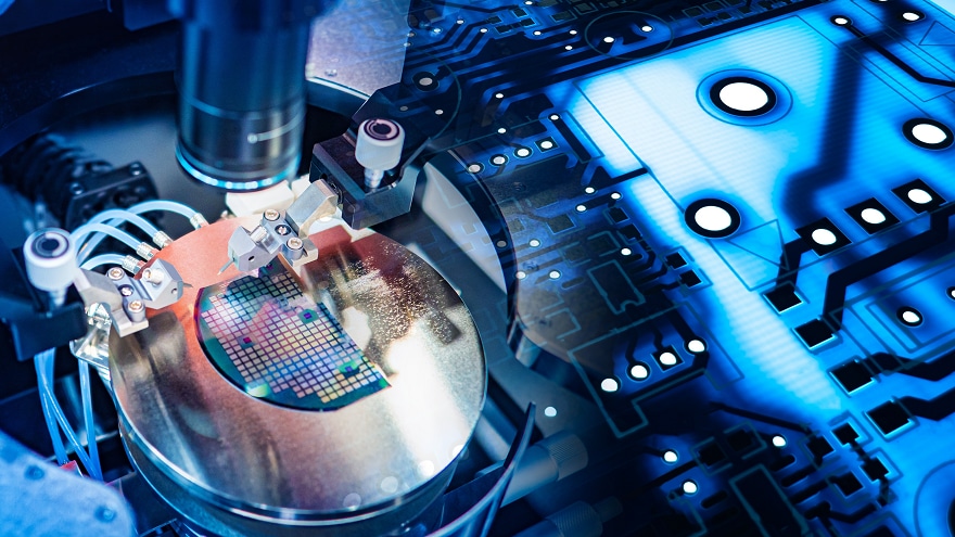
For many semiconductor teams, the microscope lab was once the place to go when something broke. That habit is changing quickly. Today, materials characterization for semiconductor R&D shapes decisions long before a device ever fails. It guides material selection, process tuning, and yield planning from the very first wafer.
The reason is easy to see. Feature sizes keep shrinking, and new materials keep entering the stack. Interfaces only a few nanometers thick now decide how a transistor, memory cell, or package performs. Waiting for a failure to study those interfaces costs time, budget, and momentum. This article explores how proactive characterization supports every stage of development. It also shares practical ways to build a faster and more dependable analysis workflow.
Why Materials Characterization for Semiconductor R&D Now Starts Upstream
Failure analysis answers one important question: what went wrong? Development teams need answers to many more questions, and they need them much earlier. Is a new barrier layer continuous? Does a deposition step leave voids? Does the etch profile match the design intent?
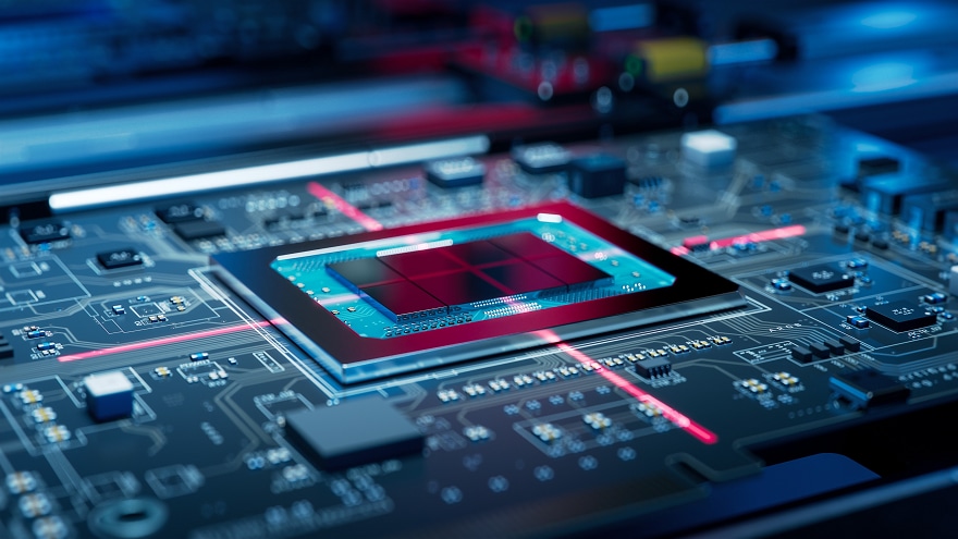
Proactive materials characterization for semiconductor R&D turns the microscope into a design partner. It supports decisions such as:
- Material screening: Compare grain structure, phase, and composition before qualifying a new film.
- Process window tuning: Check thickness, conformality, and step coverage across deposition or etch recipes.
- Interface integrity: Confirm that contacts, barriers, and bonded layers stay clean and continuous.
- Package development: Inspect solder joints, microbumps, and through-silicon vias as packaging grows more complex.
Each early insight can prevent a costly redesign later. Many teams now pair process work with electron microscopy for semiconductor development from day one. That habit shortens learning cycles and builds a solid baseline for comparison when a real failure does appear.
Cross-Section Preparation That Preserves the Real Structure
Great imaging starts with quality sample preparation. Mechanical polishing can smear soft metals, crack brittle dielectrics, and round off sharp edges. Those artifacts can look like real defects. Worse, they can hide the defects that truly matter.
Broad argon ion milling offers a gentler path. A low-energy ion beam removes material without mechanical stress, leaving a flat, wide cross section that shows true layer boundaries. Modern broad ion beam milling systems can prepare sections several millimeters wide, which lets you compare many features in a single view.
Cryogenic cooling adds another layer of protection. It limits heat damage in polymers, solders, and other temperature-sensitive materials. Flat milling can also polish a large area for crystallographic or compositional mapping. Reliable materials characterization for semiconductor R&D depends on this kind of careful preparation.
High-Resolution Imaging and Elemental Analysis at the Nanoscale
Once a clean section is ready, imaging conditions decide what you can see. Field emission SEM delivers a small, bright probe that resolves nanometer-scale features. Low accelerating voltages are especially valuable for semiconductor samples. They reduce charging on oxides and photoresists. They also keep the signal close to the surface, where thin films live.
Collecting several signals simultaneously builds a complete picture:
- Secondary electrons reveal surface topography and fine edge detail.
- Backscattered electrons highlight compositional contrast between metals and dielectrics.
- Energy-dispersive X-ray spectroscopy (EDS) maps elements across layers and interfaces.
- Electron backscatter diffraction (EBSD) shows grain orientation of interconnects and bonding layers.
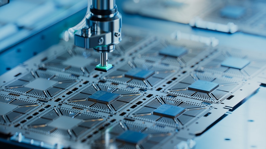
Together, these signals connect structure to chemistry. That link helps engineers explain why one recipe outperforms another. It also turns a single image into data the whole team can act on.
Scaling Materials Characterization for Semiconductor R&D with Automation
Development schedules rarely leave room for slow analysis. Your workflow needs resolution, throughput, and simple operation in balance. Hitachi High-Tech supports that balance with an integrated set of preparation and imaging tools.
The ArBlade 5000 Ion Milling System prepares cross sections up to 8 mm wide with its wide-area holder, and cryogenic versions protect heat-sensitive samples. The SU3800SE and SU3900SE Schottky FE-SEMs pair 0.9 nm secondary-electron resolution at 30 kV with an Auto Alignment Sequence. The SU3900SE accepts specimens up to 300 mm in diameter and 130 mm in height, so large substrates and packaged modules can often be mounted as is.
The compact FlexSEM 1000 II Variable-Pressure SEM suits routine checks close to the bench, offering variable-pressure imaging in a footprint only 450 mm wide. For ultrahigh-resolution work, the SU7000 FE-SEM can process, display, and save up to six signals at once for added analytical depth. For the most demanding semiconductor work, the SU8600 Ultrahigh-Resolution FE-SEM uses a cold field emission source to reach 0.7 nm secondary-electron resolution at 1 kV in deceleration mode, and its application examples include 5-nm process SRAM and 3D NAND cross sections. Each system is designed for years of dependable operation and backed by responsive service.
Let's Plan Your Next Breakthrough Together
Your semiconductor program has its own materials, deadlines, and open questions. Tell us about them. Our application specialists can help you match the right preparation and imaging tools to your goals. We can also arrange a demonstration on your own samples. When you are ready, contact our team to start building a sharper, faster view of your next device.