


Materials Characterization Techniques for Advanced Manufacturing and Research Teams
Provided by Environmental Business Division | Published: November 2, 2026
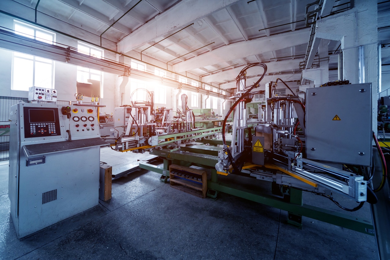
An ore that yields low recovery, a cathode batch that fails to deliver lasting performance, a component that fails technical cleanliness testing. Each of these problems starts with features too small to see by eye. Materials characterization is how mining, battery, and manufacturing teams find them. It reveals structure, composition, and defects that optical inspection often misses, and those findings shape better decisions on design, processing, and quality.
Expectations keep rising at every stage of the battery value chain. Mining teams need faster, more consistent ore analysis. Battery material developers need cathodes and anodes that hold their performance over long cycle life. Manufacturers need components that pass technical cleanliness testing and products that hold up in the field. This article covers the core techniques advanced teams use to meet those demands, following the chain from mine to finished product.
Why Materials Characterization Matters for Performance and Reliability
A material's performance depends on what happens inside it. Grain size, porosity, phase distribution, and particle shape all influence strength, conductivity, and lifespan. Small variations can lead to cracks, short circuits, or early wear.
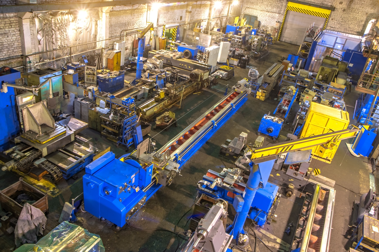
Materials characterization connects these hidden features to real-world behavior. It turns guesswork into measurable evidence. Teams can then refine their processes with data instead of trial and error.
Strong characterization helps teams answer critical questions such as:
- Which elements are present, and where are they located?
- How are particles, grains, and phases arranged?
- Where do defects, voids, or contaminants form?
- How does the structure change after processing or cycling?
Clear answers shorten development cycles. They also reduce scrap, rework, and costly surprises in the field.
Core Materials Characterization Techniques for Advanced Teams
No single method tells the whole story. Most labs combine imaging, chemical analysis, and careful sample preparation. These techniques form the backbone of modern materials characterization:
- SEM imaging: Scanning electron microscopes reveal surface detail at high magnification with excellent depth of field.
- FE-SEM imaging: A field emission source adds brightness and stability for nanoscale resolution, even at low voltages.
- Energy-dispersive X-ray spectroscopy (EDS): EDS identifies elements and maps where they sit across a sample.
- Automated particle and mineral analysis: Software pairs SEM imaging with EDS to classify thousands of particles with minimal manual effort.
- Ion milling: Broad argon ion milling exposes internal layers without the scratches or smearing that mechanical polishing can leave.
Together, these tools link what a material looks like to what it is made of. That connection is where real insight begins.
Real-World Applications in Battery Lifecycle
Each industry brings its own challenges. The right workflow depends on the sample and the question at hand.
Mining and mineral processing. Mineral liberation, grain size, and mineral associations all affect recovery. Automated material analysis turns SEM-EDS data into quantified mineral maps that geologists and metallurgists can use to tune processing.
Battery materials. Electrode particles crack, binders shift, and interfaces change during cycling. FE‑SEM imaging reveals these changes at the nanoscale. Many lithium-based materials also react quickly with air and moisture, so labs use air-protected transfer between ion milling and imaging to keep the electrode structure intact.
Product QA/QC and technical cleanliness. Residual particles on components, including battery cell parts, can cause wear, leaks, or electrical failures. Technical cleanliness is a measured property: the particle load extracted from a component is counted, sized, and checked against a defined limit. Standards such as ISO 16232 and VDA 19 guide how teams extract and measure these particles. SEM imaging enables particle size analysis, while EDS identifies elemental composition, helping teams investigate potential sources of contamination.
How Hitachi High-Tech Supports Materials Characterization
Hitachi High-Tech builds its electron-microscopy portfolio around these workflows, with systems designed for dependable, repeatable results over years of operation.
Sample preparation comes first. The ArBlade 5000 ion milling system offers both cross-section and flat-milling modes, preparing samples before they go into the electron microscope.
The SU3800SE and SU3900SE Schottky FE-SEMs combine 0.9 nm secondary-electron resolution at 30 kV with generous sample capacity. The SU3900SE accepts specimens up to 300 mm in diameter and 130 mm in height. The Auto Alignment Sequence helps operators of any skill level capture consistent images.
The FlexSEM 1000 II delivers variable-pressure SEM imaging with a footprint of only 450 mm wide, which suits single research groups and on-site labs.
AMICS (Automated Material Identification and Classification System) rounds out the workflow. It runs on a variety of Hitachi SEM and FE-SEM systems and can assist in classifying difficult phases. Behind every instrument, application specialists work closely with customers on their real samples and goals.
Build a Characterization Workflow Your Team Can Trust
Your samples, timelines, and quality targets are specific to your lab. Our application specialists can help you compare platforms, review sample needs, and plan next steps. Contact our electron microscopy team to start building a materials characterization workflow around your goals.