


Microstructure Analysis with SEM for Battery, Mining, and Manufacturing Materials
Provided by Environmental Business Division | Published: November 5, 2026
A material's microstructure is the arrangement of grains, phases, pores, and boundaries that sits far below what the eye can see. It decides how a cathode cycles, how an ore breaks during grinding, and how a cast part handles stress. Microstructure analysis measures that arrangement so teams can link processing choices to performance.
Scanning electron microscopy is one of the most practical tools for this work. It combines high-resolution imaging with chemical and crystallographic data on one platform. This article covers what microstructure analysis measures, how battery, mining, and manufacturing teams use it, and what keeps results reliable.
What Microstructure Analysis Measures
Microstructure analysis turns images into numbers. Typical measurements include:
- Grain size and shape: These affect strength, toughness, and how ions or heat move through a material.
- Phase distribution: The amount and location of each phase, which often controls hardness, conductivity, or reactivity.
- Porosity: Pore size, volume, and connectivity, which matter for electrodes, coatings, and sintered parts.
- Grain boundaries and interfaces: The places where cracks start, corrosion attacks, or layers separate.
- Inclusions and defects: Foreign particles, voids, and cracks that weaken a material.
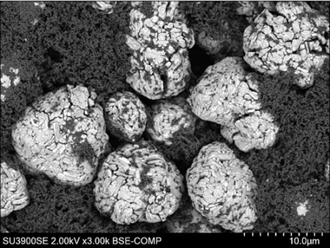
Distributions of cathode material particles and surrounding binder can be seen.
Microstructure Analysis Across Battery, Mining, and Manufacturing
Battery materials. Cathode secondary particles crack as they expand and contract during cycling. Electrode porosity controls how ions reach the active material. Cross sections imaged in an FE-SEM show particle cracking, coating uniformity, and the interface with the current collector. Hitachi High-Tech America outlines how electron microscopy supports battery development from the lab to production.
Mining and minerals. Ore texture decides how well valuable minerals can be freed and recovered. Microstructure analysis shows grain size, mineral associations, and how target minerals are locked with gangue. Backscattered electron imaging paired with EDS makes these features measurable across large areas. For mining teams, these results from SEM and Automated Material Analysis with AMICS can also feed GeoMineral AI Insights, Hitachi’s platform for connecting lab, exploration, and operations data.
Metals and manufactured parts. Grain structure, weld zones, heat-affected regions, and inclusions all influence how a part performs under load. SEM imaging of fracture surfaces and polished sections helps engineers connect a failure or a process change to its microstructural cause. A change in heat treatment, for example, often shows up first as a shift in grain size or phase balance, well before it appears in mechanical test results.
Sample Preparation and Imaging Conditions That Protect Accuracy
Microstructure analysis is only as accurate as the surface being imaged. Mechanical polishing can smear soft phases, pull out grains, and round off edges. Those artifacts can look like real porosity or cracks.
Broad argon ion milling removes material without mechanical force and leaves a flat, representative surface. Flat milling also prepares large areas for EBSD and compositional mapping. Air-sensitive battery samples need one more step, sealed transfer from preparation to the microscope, so the surface is not altered before imaging.
A 2026 Nature Energy study on stack pressure in lithium-ion pouch cells shows this in practice. Researchers moved NMC811 cathode samples under air-protected conditions to a Hitachi IM4000 Plus broad ion beam miller, then imaged the cross sections to compare particle cracking at different stack pressures.
Imaging conditions matter too. Low accelerating voltages reduce charging and keep the signal close to the surface. A stable beam current keeps contrast consistent across long mapping runs, which makes results comparable from one sample to the next.
Hitachi Solutions for Microstructure Analysis
Hitachi High-Tech offers preparation and imaging systems that work together for this kind of analysis:
- ArBlade 5000: An ion milling system with both cross-section and flat milling modes. With the wide-area holder it prepares cross sections up to 8 mm wide, and cryogenic versions protect heat-sensitive materials.
- IM4000II: An ion milling system with an Air Protection Holder Unit that keeps battery materials isolated from air on the way to the SEM.
- SU3800SE and SU3900SE: Schottky FE-SEMs with 0.9 nm secondary-electron resolution at 30 kV and an Auto Alignment Sequence for consistent imaging. The SU3900SE accepts specimens up to 300 mm in diameter.
- FlexSEM 1000 II: A compact variable-pressure SEM whose application examples include metal fracture surfaces and hydrogen storage alloys.
Hitachi application specialists also work with customers to set up preparation and imaging routines that fit their materials.
Get a Clearer View of Your Material's Structure
Whether you are tracking particle cracking, ore texture, or grain growth in a new alloy, the right preparation and imaging setup makes the difference. Contact our team to talk through your samples and plan a microstructure analysis workflow for your lab.