


What Is Materials Characterization and Who Relies on It in Battery and Advanced Manufacturing R&D
Provided by Environmental Business Division | Published: November 3, 2026
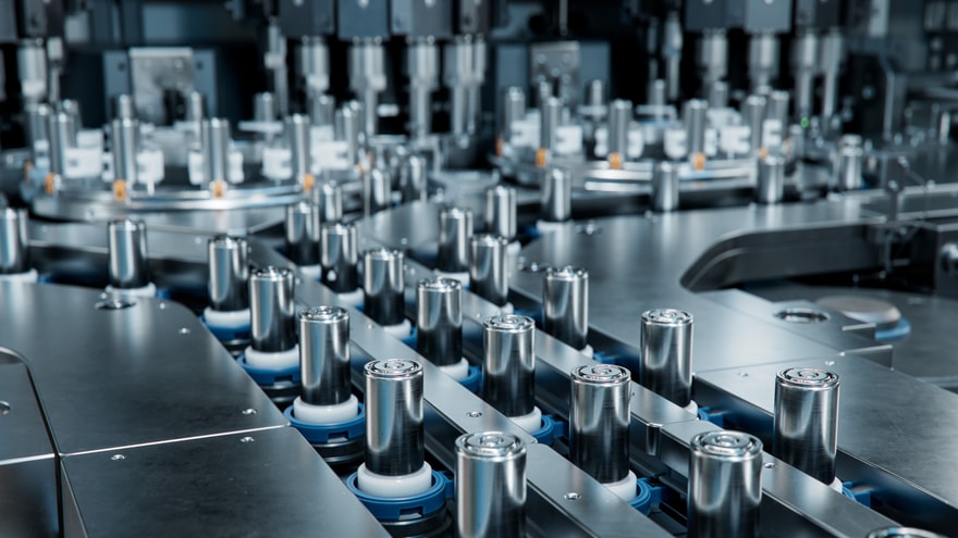
Two batches of the same cathode powder can look identical in the jar and still perform very differently in a cell. Grain size, phase distribution, porosity, and chemistry explain the gap. So what is materials characterization, and why does it matter so much in modern R&D? Put simply, it is the practice of measuring a material's structure, composition, and properties. Those measurements explain why a cathode fades, why an ore resists processing, or why a part fails early.
For battery developers, mining teams, and manufacturing engineers, characterization turns assumptions into evidence. This article explains the core idea and shows who depends on it most.
What Is Materials Characterization? A Practical Definition
Materials characterization is the systematic study of a material's structure, chemistry, and properties across length scales. It links what a material is made of with how it behaves in use. Teams use it to confirm a synthesis worked, compare suppliers, and trace defects to their source.
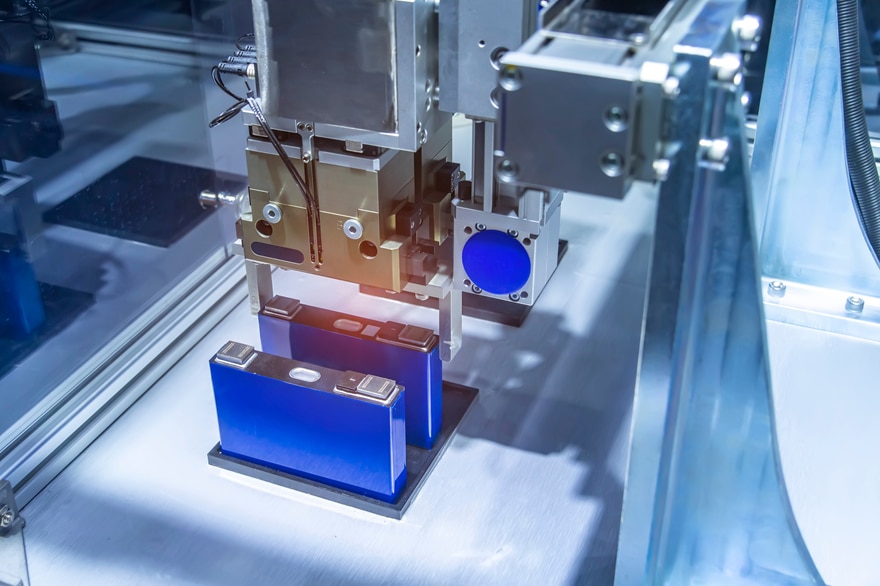
Anyone researching what is materials characterization quickly learns that it combines imaging with chemical and structural analysis. Common building blocks include:
- Scanning electron microscopy (SEM): High-magnification imaging of surface morphology, particle shape, and microstructure.
- Energy-dispersive X-ray spectroscopy (EDS): Elemental analysis inside the SEM that maps where each element sits.
- Electron backscatter diffraction (EBSD): Crystallographic mapping that reveals grain orientation and phase boundaries.
- Cross-section preparation: Polishing or milling that exposes clean internal surfaces for accurate imaging.
Modern scanning electron microscopes bring several of these methods onto one platform, so a single session can answer questions about shape, chemistry, and structure.
What Is Materials Characterization Used for in Battery R&D?
Battery performance depends on features far smaller than a human hair. Electrode coating thickness, particle cracking, binder distribution, and interphase growth all affect capacity and cycle life. For battery engineers, the answer to what is materials characterization is very practical. It is how they see these features and put numbers on them.
Field emission SEM (FE-SEM) is especially useful here. Its bright, stable beam supports sharp imaging at low accelerating voltages, which helps researchers examine beam-sensitive cathodes and separators with less charging and damage. Hitachi High-Tech America explains how electron microscopy supports battery development by connecting microstructure to cell performance.
Sample preparation matters just as much. Mechanical cutting can smear soft layers and hide true interfaces. Ion milling produces clean cross-sections that show each layer as it really is. Many battery materials also react quickly with air and moisture, so labs often use air-protected transfer between ion milling and the SEM.
How Mining and Advanced Manufacturing Teams Use Materials Characterization
Mining and geology teams ask different questions. They need to know which minerals are present and how those minerals are locked together. Those answers predict how ore will behave during crushing, flotation, and leaching. Automated mineralogy pairs backscattered electron imaging with EDS to classify thousands of particles automatically. The output includes modal mineralogy, grain size, and liberation data that guide recovery decisions.
Advanced manufacturing relies on characterization for quality and reliability. Technical cleanliness is a growing priority in automotive, aerospace, and electronics production. Standards such as VDA 19.1 and ISO 16232 guide how particles are extracted from parts and analyzed. SEM-EDS measures each particle and identifies its chemistry. Engineers can then separate a hard steel shaving from a harmless fiber. That knowledge helps them trace contamination sources before parts fail in service.
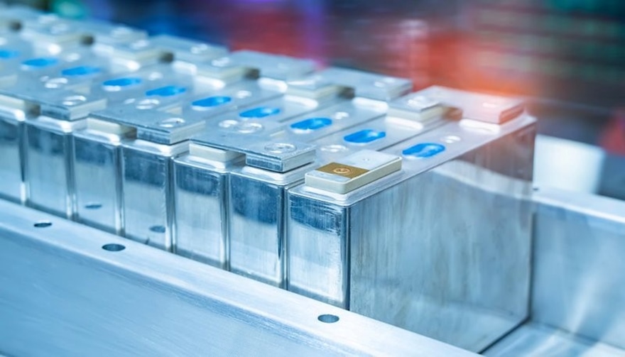
Across both fields, throughput and consistency matter. A tabletop SEM can handle fast screening near production, while larger systems support detailed studies.
How Hitachi High-Tech Supports Characterization Workflows
Hitachi High-Tech designs electron microscopes and sample preparation systems for these challenges. Key systems include:
- SU3800SE and SU3900SE: High-resolution Schottky FE-SEMs with an Auto Alignment Sequence, so operators of any skill level get consistent images. The SU3900SE accepts specimens up to 300 mm in diameter.
- FlexSEM 1000 II: A compact variable-pressure SEM only 450 mm wide with 4 nm secondary electron resolution. It suits labs and production areas where space is limited.
- TM4000PlusIII: A tabletop SEM for fast screening, with optional Recipe Control that runs imaging routines without operator input.
- AMICS: Software that automates phase identification through large-area mapping and smart EDS point placement. It runs on a variety of Hitachi SEM and FE-SEM systems and can assist in classifying difficult phases.
- IM4000II: An ion milling system whose Air Protection Holder Unit keeps air-sensitive battery samples isolated from the environment.
Hitachi instruments are known for reliability and long service life, and application specialists work with customers to shape each workflow around real samples and goals.
Let's Solve Your Next Materials Challenge Together
Your lab has its own samples, standards, and deadlines. We would love to hear about yours. Our application specialists can review your materials and recommend a workflow that fits your goals. You are welcome to ask about evaluating your own samples on the systems you are considering. Whether you study cathodes, ores, or filter particles, we are here to help you see more clearly. Contact our team today to plan a materials characterization workflow built around your research.