
Hitachi High-Tech’s
Environmental Solutions
Environmental Solutions
Environmental Products and Solutions
-
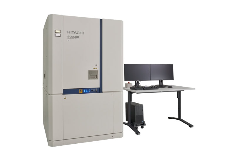
Ultrahigh-Resolution Scanning Electron Microscope SU9600 -
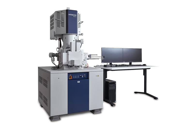
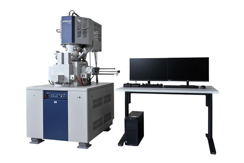
Ultrahigh-Resolution Schottky Scanning Electron Microscope SU8700 -
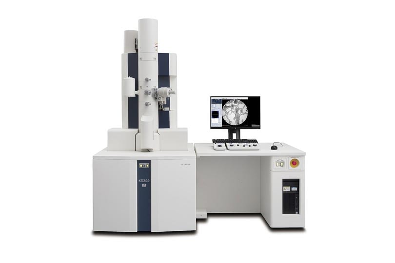
Transmission Electron Microscope HT7800 Series -
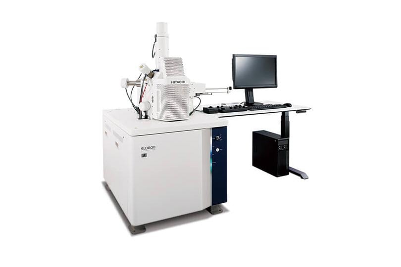
Scanning Electron Microscopes SU3800 -
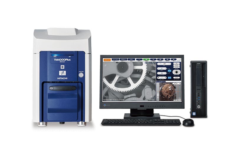
Tabletop Microscopes TM4000Plus III -
Ultrahigh-Resolution Scanning Electron Microscope SU8600 -
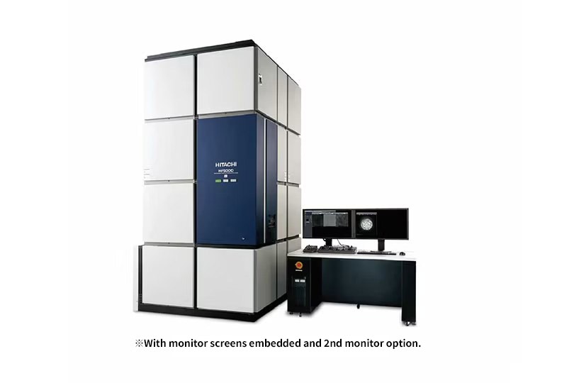
Field Emission Transmission Electron Microscope HF5000
Microscopes
Electron Microscopes (SEM/TEM/STEM)
Job Function
- Research & Development
- Manufacturing
- Quality Control
- Business Development
- Facility Management
- Testing & Diagnostics
エネルギー 製造 モビリティ 半導体 素材・化学 ヘルスケア 政府機関・研究機関
Playing an important role in driving innovation across manufacturing, research, and medical fields
Electron microscopes enable the observation of fine microstructures by using electrons, which have much shorter wavelengths than visible light. They are widely used across a broad range of fields, from inorganic materials such as metals, ceramics, and semiconductors to polymers and biological tissues.
Electron microscopes are broadly categorized into scanning electron microscopes (SEM), which observe surface structures using signals such as secondary and backscattered electrons generated by interactions between an electron beam and the sample surface, and transmission electron microscopes (TEM) and scanning transmission electron microscopes (STEM), which observe internal structures by detecting electrons transmitted through thin specimens.
Solved Issues

Decarbonization
- Supporting catalyst development
- Effective utilization of resources
- Reducing emissions

Circular Economy
- Supporting the development of eco-materials

Nature Positive
- Environmental monitoring and regulatory compliance
- Infectious disease control
- Reducing chemical emissions
- Preserving microbial balance
Related materials
Hitachi High-Tech’s Environmental Solutions