4. CD-SEM - What is a Critical Dimension SEM?
A Critical Dimension SEM (CD-SEM: Critical Dimension Scanning Electron Microscope) is a dedicated system for measuring the dimensions of the fine patterns formed on a semiconductor wafer. CD-SEM is mainly used in the manufacturing lines of electronic devices of semiconductors.
Three main CD-SEM features that differ from the general-purpose SEM:
-
CD-SEM primary electron beam irradiating to the sample has low energy of 1keV or below.
Lowering the energy of the electron beam of CD-SEM can reduce the damage to the sample due to charge-up or electron beam irradiation. -
CD-SEM measurement accuracy and repeatability is guaranteed by improving magnification calibration to the maximum extend.
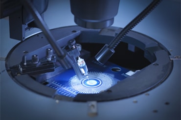
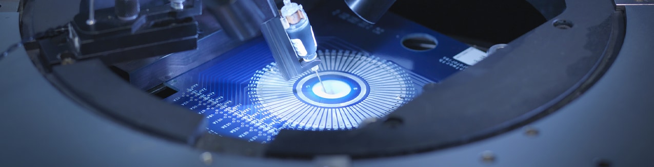
Measurement repeatability of CD-SEM is around 1% 3σ of the measurement width. - Fine pattern measurements on the wafer are automated.A sample wafer is put inside a wafer cassette (or a Pod / FOUP), which is placed on the CD-SEM. The condition and procedures of the dimensional measurement are input into a recipe* in advance. When the measurement process is started, the CD-SEM will automatically take the sample wafer out of the cassette, load it into the CD-SEM and measure the desired positions on the sample. When the measurement is finished, the wafer will be returned to the cassette.
*
Recipe:
A recipe is a program (a collection of procedures, processing methods, parameters and input data) input into manufacturing system such as CD-SEM.
Principles of measurement
CD-SEM uses the grey level (contrast) signal of the SEM image.
- First, the cursor (the position indicator) specifies the measurement position on the SEM image.
- The line profile of the specified measurement position is then obtained. A line profile is basically a signal that indicates changes in topographical profile of the measured feature.
- A line profile is used to obtain the dimensions of a specified position. CD-SEM calculates the dimensions automatically by counting the number of pixels in the measurement area.
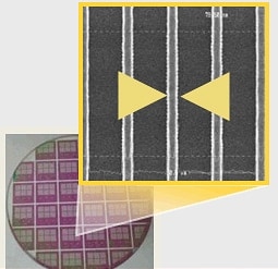
CD-SEM image
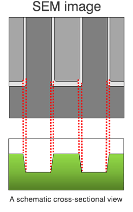
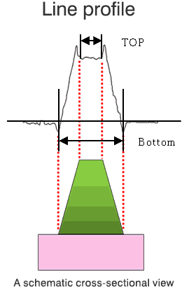
An example of SEM image obtained by CD-SEM is shown below. Fig.4-1 shows a line profile drawn on top of an SEM image of a photoresist line. The relationship between the cross-sectional view of the photoresist line and the SEM image is shown in Fig.4-2.
Furthermore, the relationship between the line cross-section and its line profile is shown in Fig.4-3.

That is, the image in Fig.4-1 gives the line profile, which in turn gives the line width. If the line cross-section is in the shape of a trapezoid as in Fig.4-3, the width at the top and bottom will be different. In that case, the measurement position will be specified in the recipe. In addition, the desired height position can also be specified.
Measurement process
Critical dimension measurement is mainly performed in the following operations of the wafer fabrication process.
- Critical dimension measurement of photoresist pattern after development
- Measurement of the contact hole diameter / via-hole diameter and the wiring width after etching
Products
Hitachi Advanced High Resolution CD-SEM
Since Hitachi launched its first CD-SEM in 1984, it has been consistently following the critical dimension measurements method based on the SEM image, evolving and maintaining excellent measurement repeatability for over 30 years. While maintaining high resolution that is compatible with the semiconductor microfabrication trend, Hitachi is providing robust CD-SEM demonstrating a high availability and incorporating various new functions required by the manufacturing and development lines meeting customer's needs.
Introducing the product lineup of advanced high resolution Critical Dimension - Scanning Electron Microscope (Hitachi CD-SEM)
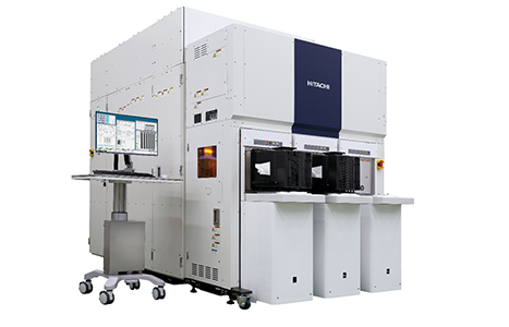
High-Precision Electron Beam Metrology System GT2000
CD-SEM to meet the needs of semiconductor devices development and mass production in High-NA EUV generation
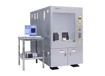
Advanced CD Measurement SEM CS4800
A sustainable CD measurement solution to a wide range of 4, 6, and 8 inch wafer Fabs
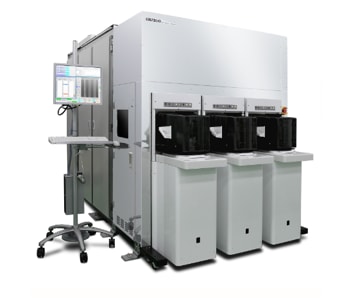
Advanced CD Measurement SEM CG7300
For the EUV era device production – High Reliability CD-SEM
Advanced CD Measurement SEM CG6300
The newly developed Advanced CD Measurement SEM CG6300 (HITACHI CD-SEM) will offer higher resolution with a fully renewed electron optical system along with improved metrology repeatability and image quality.
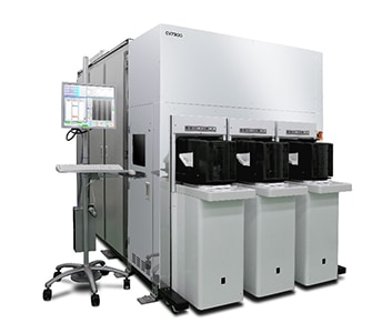
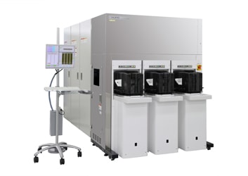
High Voltage CD-SEM CV7300
An in-line measurement system with 60kV acceleration voltage
Page 4 of 7
Related Contents
What are semiconductors?

Semiconductor manufacturing