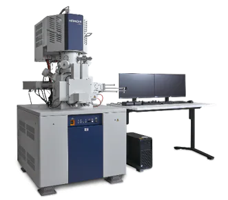
Ultrahigh-Resolution Scanning Electron Microscope SU8600
The SU8600 brings in a new era of Ultrahigh-Resolution cold-field emission scanning electron microscopes to the long-standing Hitachi EM lineup. This revolutionary CFE-SEM platform incorporates multifaceted imaging, automation, increased system stability, efficient workflows for users of all experience levels, and more.
* The device photograph shows configuration with optional items.
Features
Ultrahigh-Resolution
Hitachi’s high-brightness cold field emission source provides Ultrahigh-Resolution images even at Ultra-low voltages.
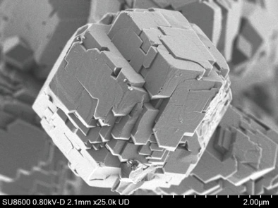
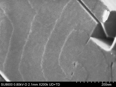
Specimen courtesy of Dr. Yoshihiro Kamimura,
National Institute of Advanced Industrial Science and
Technology (AIST), Japan
Left: RHO-type Zeolite particle at low-kV. In order to reveal fine steps structure on surface, the image was acquired at 0.8 kV of landing voltage. This allows the very fine structure of surface steps to be clearly visible (image on right).
A Smart Detection System for Low Voltage BSE Imaging
Cross section image of 3D NAND;
Oxide layer and Nitride layer of capacitor are easily distinguishable in the image due to BSE detection capability.
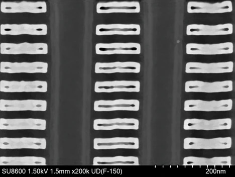
Fast BSE Imaging : New Out-Column Crystal Type BSED (OCD)
By using new Out-Column Crystal Type BSED (OCD)*, image acquisition time was less than ONE SECOND, yet lower layer interconnect and Fin FET structure of SRAM are clearly visible.
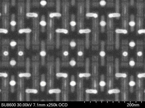
* Option
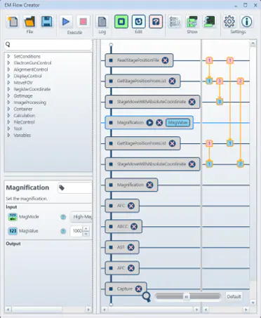
Enhanced User Experience with Advanced Automation
The “EM Flow Creator“ software option allows users to configure repeatable SEM operation sequences.
Various SEM functions can be assembled in the EM Flow Creator’s window by a drag-and-drop method and then saved as a recipe for later use.
Once a recipe is configured, automated data collection under the set conditions can be performed with high accuracy and repeatability.
Flexible Interface
Dual monitor configuration supports a flexible and highly efficient workspace. Display and save 6 signals simultaneously in order to acquire more information in less time.
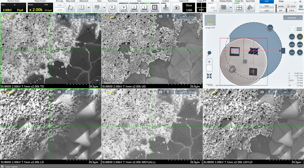
1, 2, 4 or 6 signals, including the chamber scope(*) or SEM MAP, can be displayed simultaneously on a single monitor. By adding a second screen, the dual-monitor configuration supports enhanced productivity plus expanded workspace and allows the operation panel to be customized with submenus positioned anywhere on either screen.
Specifications
| Electron Optics | Secondary Electron Image resolution | 0.6 nm@15 kV |
|---|---|---|
| 0.7 nm@1 kV (*1) | ||
| Magnification | 20 to 2,000,000 x | |
| Electron Gun | Cold cathode field emission gun with anode heating system | |
| Accelerating Voltage | 0.5 to 30 kV | |
| Landing Voltage(*1) | 0.01 to 20 kV | |
| Standard Detectors | Standard Detectors | Upper Detector (UD) with ExB filter: SE/BSE signal mixing function |
| Lower Detector (LD) | ||
| Option Detectors | Top Detector (TD) | |
| In-Column Middle Detector (IMD) | ||
| Out-Column Crystal Type BSED (OCD) | ||
| Semiconductor Type BSED (PD-BSED) | ||
| Cathodoluminescence Detector (CLD) | ||
| STEM Detector | ||
| Optional Accessories(*2) | Energy Dispersive X-ray Spectrometer (EDS) | |
| Electron Backscattered Diffraction Detector (EBSD) | ||
| Specimen Stage | Stage Control | 5-axis Motor Drive |
| Movable Range | ||
| X | 0 to 110 mm | |
| Y | 0 to 110 mm | |
| Z | 1.5 to 40 mm | |
| T | -5 to 70° | |
| R | 360° | |
| Specimen Chamber | Specimen Size | Max. φ150 mm(*3) |
(*1) with deceleration mode
(*2) Mountable Detectors
(*3) please contact for information on larger sizes
Citations
 Powered by Bioz
Related Information

Hitachi High-Tech Social Media