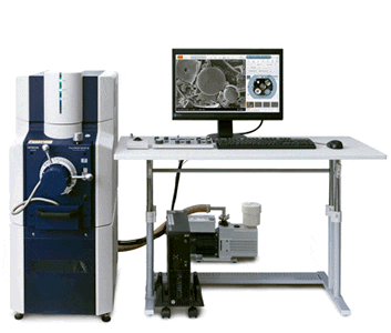
Scanning Electron Microscope FlexSEM 1000 II
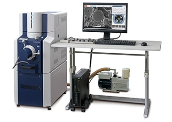
The FlexSEM 1000 II VP-SEM combines innovative features with an intuitive interface, to deliver flexibility in a powerful, automated, lab-friendly package. Cutting-edge technology provides unrivaled imaging performance, even in variable-pressure environments, a feature typically available in full-sized SEMs.
The FlexSEM will change your view of electron microscopy!
Features
-
The FlexSEM 1000 II Scanning Electron Microscope features new electron optics and signal detection capabilities. The system provides exceptional imaging and analytical performance in a lab-friendly configuration. The FlexSEM utilizes a flexible and adaptable design. It can be installed in limited office, laboratory, or multi-use spaces. Engineered for both novice and expert microscopist, for a wide range of applications. From biological to advanced material specimens, this microscope will expand your analyses as well as your expectations.
Compact & High-Performance Column
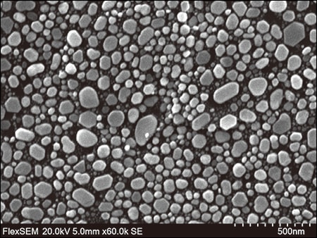
Best-in-class resolution in a compact system. The FlexSEM employs a newly designed electron optics with a reliability-proven high-sensitivity detector, achieving imaging at 4 nm.
Compact and high-performance electron optics
Equipped with a low-aberration objective lens, providing high resolution in a compact body.
SE image resolution: 4.0 nm
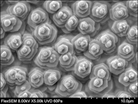
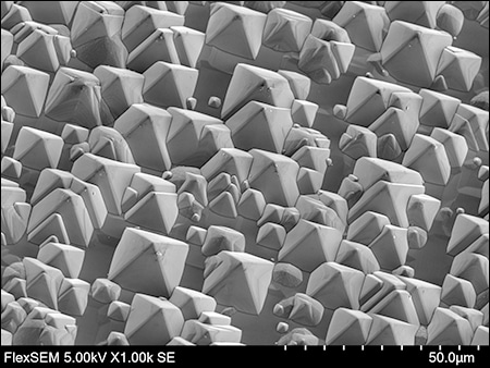
Accelerating voltage: 20.0 kV, Magnification: 60,000x BSE image resolution: 5.0 nm
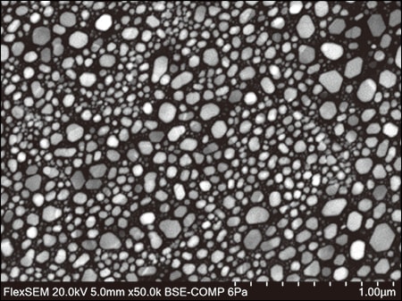
Accelerating voltage: 20.0 kV,
Magnification: 50,000x , Vacuum: 6 Pa
Specimen: evaporated Au particlesNew generation ultra variable-pressure detector (UVD-II)*1
The UVD-II, a ultra variable-pressure detector with improved signal detection capability, provides a signal-to-noise ratio approximately 1.5 times higher than the previous-generation UVD.
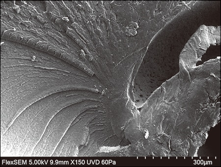
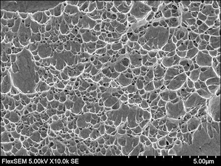
Accelerating voltage: 5.0 kV,
Magnification: 150x
Signal: UVD-II
Specimen: resin fracture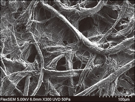
Accelerating voltage: 5.0 kV,
Magnification: 300x
Signal: UVD-II
Specimen: paper filter*1 Optional
New & Improved Auto Functions
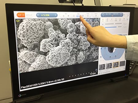
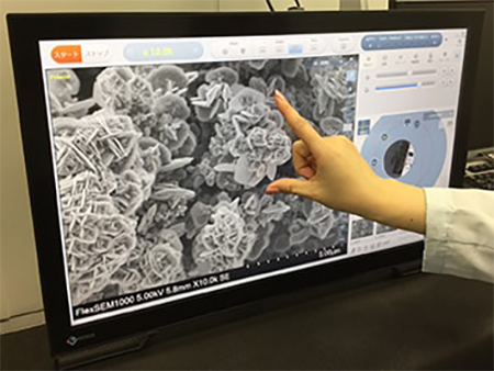
The user interface is easy to operate. With various automated functions, high-quality and quick data acquisition can be accomplished regardless of user experience. The system can be used with touch panel screen option.
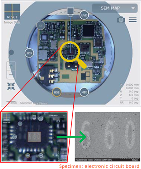
Intuitive Sample Navigation
SEM MAP helps to locate regions of interest quickly, and delivers accurate correlated optical and SEM images using only one click. Optical and EM correlation function (SEM MAP) is fully integrated into the GUI.
-
The FlexSEM 1000 II's compact design (only 450 mm wide) minimizes the system's footprint. The separable unit design allows it to fit in a variety of spaces. The entire system operates using a standard wall outlet, making installation and facility management easy.
FlexSEM 1000 II -
The newly developed electron optics and Ultra-Variable-Pressure Detector (UVD) enable superior imaging of specimen surfaces at low accelerating voltages and low vacuum conditions. The continous bias technology allows users to achieve high signal level at all accelerating voltages.
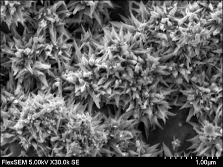
Accelerating voltage: 8.0 kV,
Magnification: 5,000x
Specimen: abalone's shell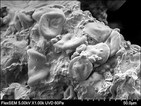
Accelerating voltage: 5.0 kV,
Magnification: 1,000x
Specimen: pancake -
The user-friendly GUI provides fast and accurate Auto Focus Control (AFC) and Auto Brightness and Contrast Control (ABCC) algorithms. These functions execute in only 5 seconds to enable optimized imaging performance with minimal time and effort.
-
The "SEM MAP" function allows for effortless navigation across the entire specimen. Navigate across your sample with the use of an optical camera, and deliver accurate correlated optical and SEM images using only a single click.
-
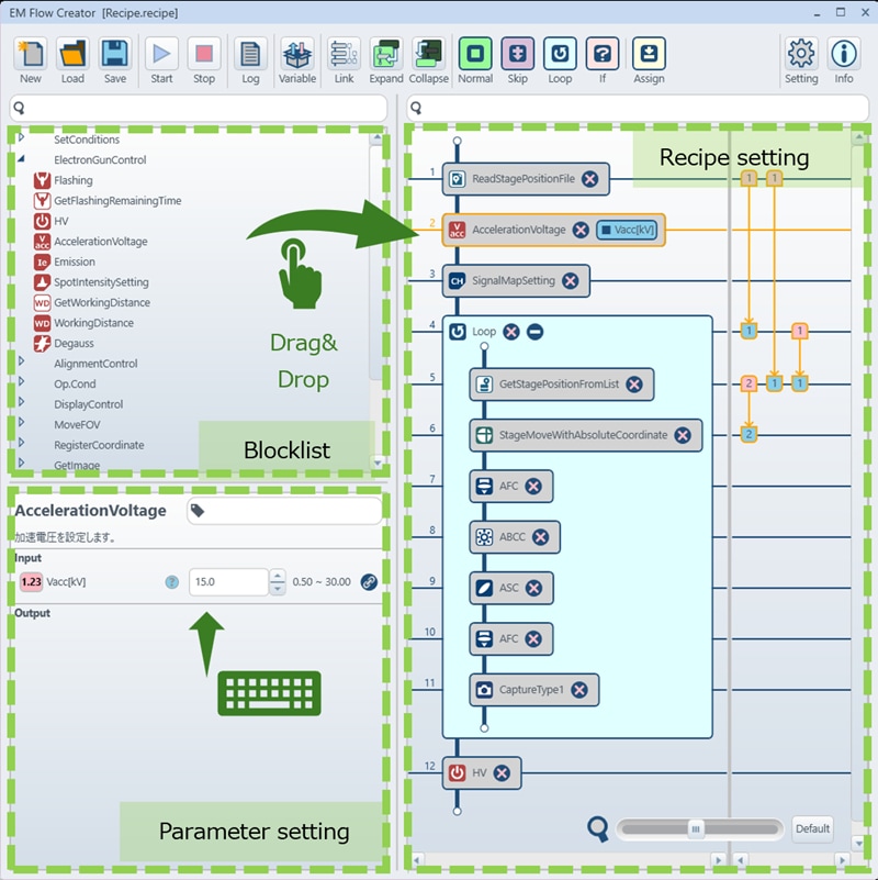
The EM Flow Creator is available to support automation of operations such as sequential image capture. A series of observation steps can be created by setting parameters, such as magnification, stage position, focus, and contrast adjustment, into blocks that can be combined, thus allowing the creation of customized recipes. Recipes can be created by dragging and dropping blocks into an arrangement like a flowchart. Automatic observation is possible by executing a created recipe.
Application Data
Materials Science
Magnification: 1,000x
Specimen: solar cell
Magnification: 10,000x
Specimen: fracture surface of metal
Magnification: 30,000x
Specimen: hydrogen storage alloy
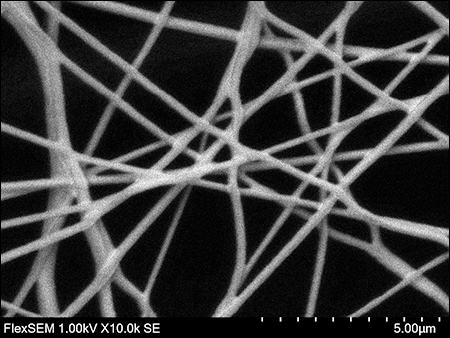
Magnification: 10,000x
Specimen: nanofiber
Sample courtesy of Nafias corporation
Biology
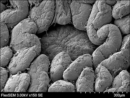
Magnification: 150x
Specimen: Peyer's patch of small intestine
Sample courtesy of associate professor Daisuke Koga,
Department of Microscopic Anatomy and Cell Biology,
Asahikawa Medical College
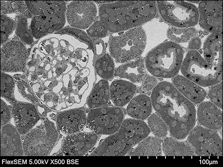
Magnification: 500x
Specimen: kidney section of a mouse (resin-embedded)
Semiconductors
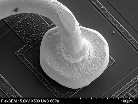
Magnification: 500x(UVD used)
Specimen: wire bonding
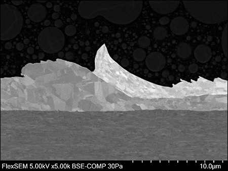
Magnification: 5,000x (Ion milling used)
Specimen: Au bonding
Specifications
| Items | Description | |
|---|---|---|
| Electron Optics | Secondary Electron resolution(*1) | 4.0 nm (Accelerating voltage 20 kV, WD = 5 mm, high-vacuum mode ) |
| 15.0 nm (Accelerating voltage 1 kV, WD = 5 mm, high-vacuum mode ) | ||
| Backscattered electron resolution(*1) | 5.0 nm (Accelerating voltage 20 kV, WD = 5 mm, VP mode) | |
| Accelerating Voltage | 0.3 kV to 20 kV | |
| Magnification | 6x to 300,000x (magnification ratio of image) (*2) 16x to 800,000x (magnification ratio of display) (*3) |
|
| Pressure Range | Variable pressure range | 6 to 100 Pa (13 steps) |
| Electron optics system | Electron gun | Precentered cartridge type tungsten hairpin filament |
| Specimen Stage | X | 0 to 50 mm |
| Y | 0 to 40 mm | |
| Z | 5 to 33 mm | |
| R | 360° | |
| T | -15° to +90° | |
| Maximum observable range | 64 mm in diameter (combined with Rotation) (*4) | |
| Motor drive | 3-axis (X, Y, R) | |
| Dimension | Main unit | 450 (W) × 795 (D) × 690 (H) mm |
| Power box | 450 (W) × 640 (D) × 450 (H) mm | |
| Accessories | Detector | Ultra variable-pressure detector (UVD-II ) |
| Energy dispersive X-ray spectrometer (EDS) | ||
| Specimen stage/holder | Multi sample holder | |
| STEM holder | ||
| Software | Multi Zigzag | |
| Hitachi map 3D | ||
*1 When the main unit and power box are connected.
*2 Magnification is defined with a display size of 127 mm × 95 mm (4 × 5 picture size).
*3 Magnification is defined with a display size of 509.8 mm × 286.7 mm (1,920 × 1,080 pixels).
*4 When using the standard holder.
Citations
 Powered by Bioz
Hitachi FIB Application Data
This journal addresses a wide range variety of research papers and useful application data using Hitachi science instruments.
Photo collections of beauty of metals, minerals, organisms etc. reproduced by the electron microscope and finished more beautifully by computer graphic technology.
Related Product Categories
Related Information

Hitachi High-Tech Social Media