Semiconductors

The "minimization of design" rule for semiconductor device manufacturing is advancing at a remarkable rate. Recent advancements in techniques make it possible to control device structures at an atomic level. To this end, electron microscopy has become an indispensable technique allowing high-resolution imaging with a quick turnaround time. The electron microscope is able to cover a very wide scale range for evaluating everything from the packaged device to the atomic level gate structure. Hitachi High-Tech offers highly advanced in-line and off-line analysis systems for semiconductor device development, manufacturing, failure analysis and quality assurance. We produce a wide range of electron microscope solutions including the world's leading FE-SEM, FIB-SEM, and TEM systems.
Analysis field of semiconductor devices

In the semiconductor device manufacturing process, electron beam based systems are widely used for developing next generation semiconductor devices, and for QTAT process control for improving manufacturing yield.
Key analysis for FEOL & BEOL
- Critical dimension measurement
- Pollution, particle analysis
- Voltage contrast
- Individual transistor electrical measurement
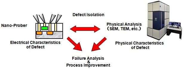
A wide variety of electron beam based systems are used for analyzing the source of a device failure and improving its manufacturing process. QTAT failure analysis is in demand for improving device quality and building a reliable partnership with customers.
Key points of interest for failure analysis:
- Pollution, particle analysis
- Metal interconnect line Net localization
- Voltage contrast
- Individual transistor electrical measurement
- Critical dimension measurement
- Diffusion region analysis
For chip level analysis
| Purpose |
|
|
|
|
|---|---|---|---|---|
| Image Example |
|
|
|
|
| Product |
For PCB & Package-Level Analysis
| Purpose |
|
|
|
|---|---|---|---|
| Image Example |
|
|
|
| Product |
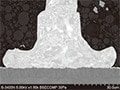
Condition Analysis of a device soldered on PCB
Requirement
- Large size stage & variable pressure mode for printed circuit board
Target Device
- Device on the printed circuit board
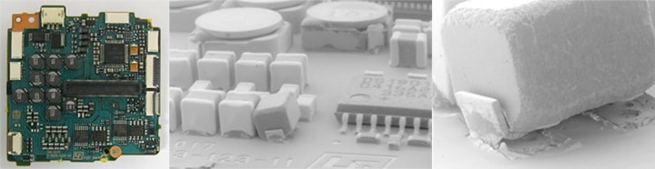
Solution
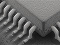
Wire Bonding Analysis
Requirement
- High precision cross section milling without mechanical stress, and high quality SEM imaging at variable pressure mode
Target Device
- Packaged device
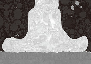
Solution
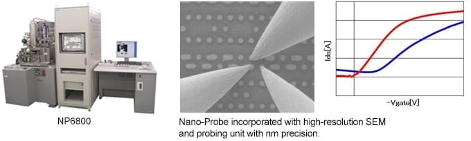
Voltage Contrast and Current Imaging
Requirement
- Rapid, clear and easy voltage contrast and current image observation
Target Device
- Smaller than 2x nm Logic, DRAM, and NAND-FLASH
Target detection
- Electrical open and leakage
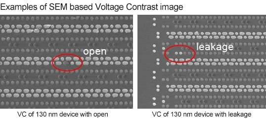
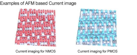
Solution
SEM:
Electrical Characteristics Measurement
Requirement
- Capability of 10 nm beyond device measurement
- Clear and high resolution SEM live image without device damage
Target Device
- Beyond 10 nm design node Logic, DRAM, and NAND-FLASH
Target characteristics
- Static characteristic, AC characteristic, & Electron Beam Absorbed Image
Solution
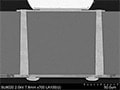
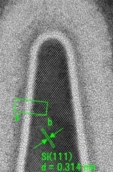
TEM Specimen Preparation
Requirement
- End point detection at cross-section milling
- Easy and high quality cross-section sample preparation without damage or curtaining effects for high resolution TEM analysis
Target Device
- Beyond 20 nm design node Logic, DRAM, and NAND-FLASH
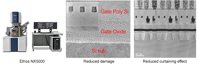
Solution
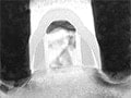
TEM/STEM Based CD Measurement
Requirement
- Ultrahigh-Resolution TEM/STEM for CD measurement
Target Device
- Beyond 10 nm design node Logic, DRAM, and NAND-FLASH
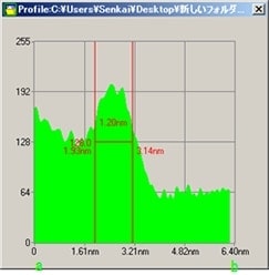
Solution
TEM:
Analysis of Diffusion Area
Requirement
- Rapid TEM analysis for detecting low-concentration impurity elements
- Rapid AFM analysis for confirming diffusion area
Target Device
- Beyond 20 nm design node Logic, DRAM, and NAND-FLASH
Target element
- Boron, Arsenic, and Phosphor for Source-Drain
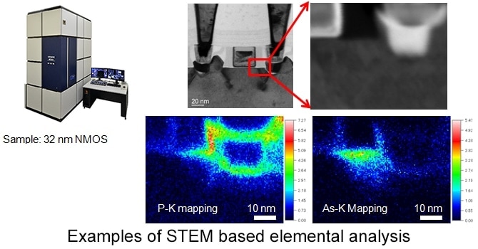
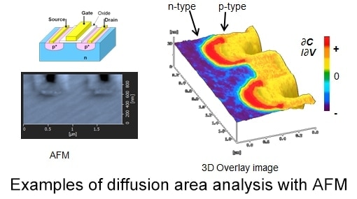
Solution
TEM:
Related topics

“S.I.navi” is Hitachi Membership Site for analytical instruments users.
“S.I.navi” provides helpful information for daily analysis.


Hitachi High-Tech Social Media