
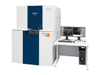
Focused Ion and Electron Beam System & Triple Beam System NX2000
Toward the ultimate TEM sample preparation system
FIB-SEM systems have become an indispensable tool for characterization and analysis of the latest technologies and high performance nano-scale materials. An ever-increasing demand for ultrathin TEM lamellas without artifacts during FIB processing require the best in ion and electron optics technologies.
Hitachi's NX2000 high performance FIB and high resolution SEM system with its unique sample orientation control* and triple beam* technologies, supports high throughput, and high quality TEM sample preparation for cutting edge applications.
* Option
Features
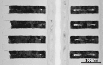
High contrast, real-time SEM end point detection allows ultrathin TEM sample preparation of sub 20 nm devices.
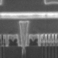
Real-time SEM monitoring during FIB milling
Sample: NAND flash memory
Accelerating voltage: 1 kV
FOV: 0.6 µm
Micro sampling* and high precision positioning mechanism* enable sample orientation control for Anti-Curtaining Effects (ACE function) and uniformly-thick lamellas.
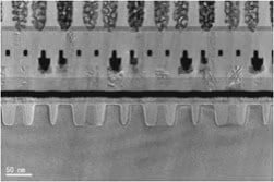
Triple Beam system* Triple beam configuration for Ga FIB-induced damage reduction.
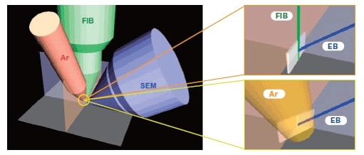
EB: Electron Beam
FIB: Focused Ion Beam
Ar: Argon ion beam
Specifications
| FIB column | |
|---|---|
| Resolution (SIM) | 4 nm@30kV, 60 nm@2kV |
| Acceleration voltage | 0.5 kV - 30 kV |
| Beam current | 0.05 pA - 100 nA |
| FE-SEM column | |
| Resolution | 2.8 nm@5kV, 3.5 nm@1kV |
| Acceleration voltage | 0.5 kV - 30 kV |
| Electron source | Cold cathode field emission source |
| Detector | |
| Standard detector | Upper/Lower SED & BSED |
| Stage | X: 0 - 205 mm Y: 0 - 205 mm Z: 0 - 10 mm R: 0 - 360° infinite T: -5 - 60° |
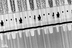
The NANOMESH grid for FIB processing alleviates redeposit effects for high quality lamella preparation.
Numerous locations for mounting lamellae allows for high precision sample preparation and material features for better analysis.
Special accessories (Optional)
- Ar/Xe ion 3rd column
- Micro-sampling System
- Multi-gas injection system
- Double tilt system
- Swing function ( for Ar/Xe ion 3rd column)
- TEM sample preparation wizard
- Automatic TEM sample preparation software
- CAD navigation software
- Linkage software with defect inspection instruments
- Air protection holder
- Cooling holder
- Plasma cleaner
- EDS (Energy Dispersive x-ray Spectroscopy) system
Application Data
Semiconductor
3D reconstruction from serial section SEM images
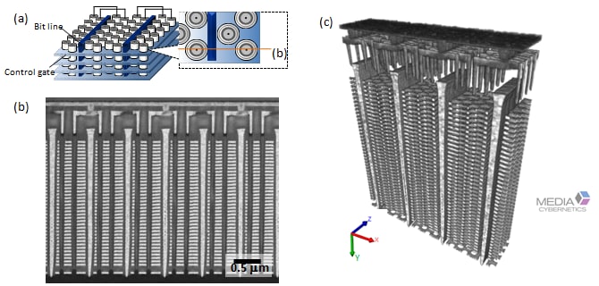
Specimen: 3D NAND flash memory
(a) Schematic view
(b) Cross-sectional BSD image (Accelerating voltage : 2 kV)
(c) 3D reconstructed image (Volume rendering)
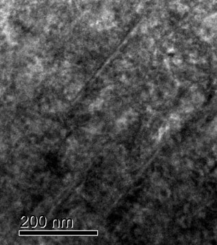
Curtain effect free lamella preparation using double tilt system
Observation: HF-3300 Cold FE-TEM (Accelerating voltage : 200 kV)
High-precision site-specific lamella preparation
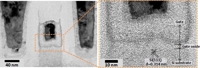
Observation: HF-3300 Cold FE-TEM (Accelerating voltage : 200 kV)
High-quality lamella preparation with in-situ Ar ion milling
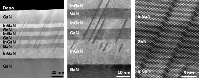
Final milling: 1 kV Ar
Observation: HD-2700 Aberration -corrected STEM (Accelerating voltage : 200 kV)
Material Science
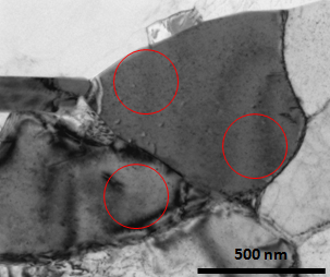
High-quality lamella preparation with in-situ Ar ion milling (1)
30 kV FIB
1 kV Ar
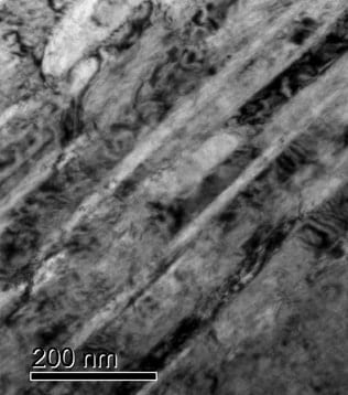
Specimen: Zirconium
Observation: HF-3300 cold FE-TEM (Accelerating voltage: 300 kV)
High-quality lamella preparation with in-situ Ar ion milling (2)
30 kV FIB
1 kV Ar
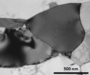
Specimen: Aluminium
Observation: HF-3300 cold FE-TEM (Accelerating voltage: 300 kV)