


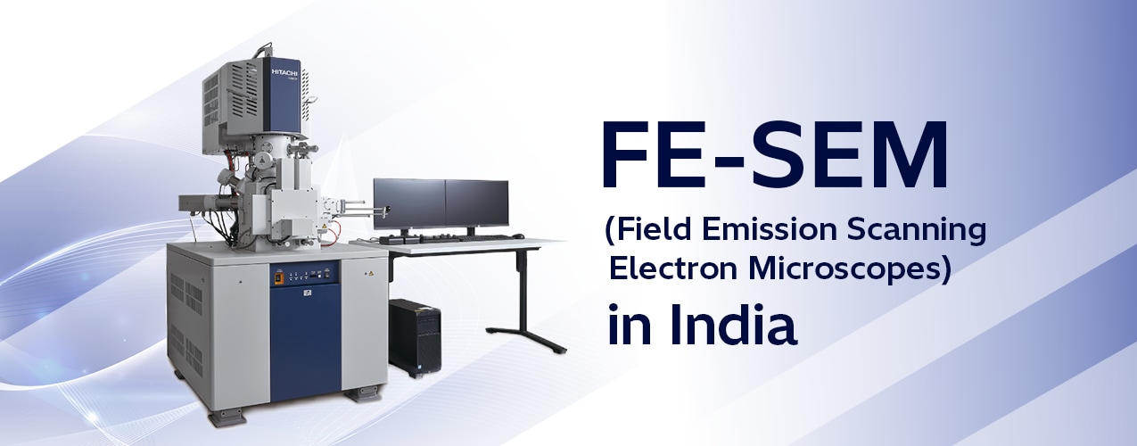
Hitachi SU8600 Field Emission Scanning Electron Microscope
FE-SEM (Field Emission Scanning Electron Microscopes) in India
Enable ultra-high-resolution imaging, faster failure analysis, and smarter research
As feature sizes in advanced semiconductor nodes scale down to sub 6nm levels, high-resolution imaging and fast, repeatable analytical testing have become critical. Supporting India’s expanding semiconductor ecosystem, Hitachi High-Tech’s FE-SEM portfolio – including SU8600, SU8700, and SU7000 combines high-stability field emission sources, intelligent automation software, and advanced imaging capabilities to help organizations achieve higher productivity, accuracy, and process control.
Main industries we support
Semiconductor and electronics
Accelerate defect review, failure analysis, process characterization, yield improvement, and advanced packaging inspection for next-generation semiconductor technologies.
Battery and energy storage
Detailed characterization of battery electrodes and separators enables analysis of micro-cracking, binder distribution, and conductive network integrity. Cross-sectional imaging and nanoscale defect inspection support battery performance optimization.
Automotive and advanced manufacturing
Ultra-high resolution of heavy and complex physical components for large scale specimen observation without destructive downsizing and high definition secondary and backscattered electron (SE/BSE) imaging to map nanoscale surface micro-cracks, analyze fracturing behavior and material integrity.
Pharmaceuticals and medical devices
Analysis of pharmaceutical particles, drug delivery systems, and biomaterials enable evaluation of particle morphology, Active Pharmaceutical Ingredients (API) distribution, and formulation uniformity. Variable pressure imaging supports stable observation of delicate, non-conductive, and hydrated samples accelerating quality control, regulatory compliance, and drug delivery validation.
Academia and research institutes
Versatile imaging of conductive, insulating, and delicate samples without conductive coating supports multi-disciplinary research across materials science, life sciences, polymers, and geology. Intuitive operation, high-throughput workflows, and high-stability CFE technology maximize shared facility utilization while minimizing downtime and maintenance costs.
Why choose Hitachi’s FE-SEM?
Keep pace with semiconductor miniaturization with ultra-high-resolution imaging, intelligent automation, and high-throughput analysis. Designed for sub-6nm semiconductor inspection, failure analysis, process control, and materials characterization, Hitachi FE-SEM systems deliver sub-nanometer resolution, exceptional stability, and highly repeatable results.
Advanced automation and streamlined workflows accelerate defect inspection, root cause analysis, and nanoscale characterization, helping semiconductor fabs, testing laboratories, and research institutions improve productivity while reducing time to insight. The result is faster decision-making, higher yield optimization, and greater confidence in advanced manufacturing and R&D applications.
Key Technologies Powering Next-Generation FE-SEM Performance
High-resolution imaging alone is not enough for advanced-node inspection. Hitachi FE-SEM systems combine precision electron optics, intelligent automation, and specialized detectors to deliver superior imaging, analytical accuracy, and workflow efficiency:
- Cold Field Emission (CFE) Technology – exceptional beam brightness and stability
- ExB and SuperExB Signal Filtration – precise SE/BSE signal separation
- Advanced Control Software (ACS) – automated multi-point recipes
- EM Flow Creator – recipe-driven workflow automation
- Advanced Detector Configurations – metrology and failure analysis
Cold Field Emission (CFE) Technology
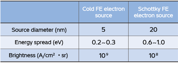
As shrinking feature sizes in semiconductor ecosystem push devices beyond the limits of conventional inspection, Hitachi's proven Cold Field Emission (CFE) technology delivers the resolution, stability, and analytical precision needed for advanced process control and failure analysis. Developed from over 50 years of CFE innovation, it provides sub-nanometer imaging at ultra-low (0.5-1.5 kV) accelerating voltages, enabling clear visualization of nanoscale structures while minimizing beam damage to sensitive semiconductor materials.
With exceptional beam brightness, long-term emission stability, and high probe current performance, CFE technology enables faster defect inspection, more accurate metrology, and highly repeatable nanoscale characterization for advanced semiconductor manufacturing and R&D.
ExB and SuperExB Signal Filtration
As semiconductor structures become increasingly complex, precise signal separation is critical for accurate semiconductor inspection, metrology, and failure analysis. Hitachi's ExB and SuperExB Signal Filtration technology uses orthogonal electric and magnetic fields positioned above the objective lens to selectively filter electrons without affecting the primary beam trajectory.
The SuperExB Signal Mixing Layout allows precise control of secondary electron (SE) and backscattered electron (BSE) signals through conversion electrode voltage adjustment, enabling optimized topographic and material contrast with exceptional sensitivity to atomic number differences. Combined with the ability to display up to six imaging channels simultaneously, users can efficiently analyze interconnect routing, via structures, step coverage, and deep trench features in a single acquisition, accelerating advanced semiconductor process development and defect characterization.
Advanced Control Software (ACS)
Increase throughput and improve measurement consistency with Advanced Control Software (ACS), designed to automate complex SEM inspection, metrology, and failure analysis workflows. ACS bridges the gap between manual analysis and fully automated recipe processing, enabling engineers to create, save, and execute multi-step inspection routines with minimal operator intervention.
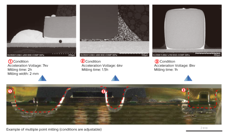
By storing pre-programmed sample coordinates, Automated Recipe Processing reduces setup time and streamlines repetitive inspection tasks. Multi-Position & Condition Profiling allows multiple imaging conditions, such as high accelerating voltage for lower-layer interconnect contrast and low landing voltage for sensitive surface structures, to be executed automatically within a single run. ACS also supports unattended acquisition of cross-sectional views, tilted views, and multi-field-of-view arrays, helping semiconductor fabs and analytical laboratories improve productivity, repeatability, and workflow efficiency.
EM Flow Creator
Improve productivity and measurement consistency with EM Flow Creator, an advanced workflow automation platform for SEM inspection and analysis. By converting complex procedures into automated, recipe-based workflows, it enables unattended operation, intelligent feature recognition, and standardized data acquisition. The result is faster throughput, reduced operator workload, and more repeatable results for semiconductor inspection, failure analysis, metrology, and materials characterization. EM Flow Creator is available across Hitachi SEM platforms, including the SU8700.
Advanced Detector Configurations for Metrology & Failure Analysis
As advanced-node scaling increases device complexity, comprehensive signal detection is essential for accurate metrology, defect inspection, and failure analysis. Hitachi FE-SEM systems support a range of advanced detector configurations that deliver complementary topographic and compositional information, enabling deeper insight into semiconductor structures and materials.
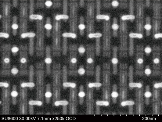
The Upper Detector (UD) with ExB Filter combines high-resolution surface imaging with material contrast analysis, while the Lower Detector (LD) provides optimized topographic imaging at extended working distances. The In-Column Middle Detector (IMD) delivers high-sensitivity atomic number contrast (Z-contrast) imaging at high scan speeds, supporting rapid characterization of complex device structures. For advanced semiconductor applications, the Out-Column Crystal Type BSED (OCD) enables acquisition in less than a second of deep-layer interconnect and FinFET routing information, helping engineers accelerate process development, yield improvement, and root-cause failure analysis.
| Capability | Technical Specification | Advantage |
|---|---|---|
| Electron Source Gun Type | Cold Cathode Field Emission (CFE) gun with localized flash anode heating system | Sub-nanometer clarity |
| Secondary Electron (SE) Resolution | 0.6 nm at 15 kV 0.7 nm at 1 kV landing voltage |
High-fidelity surface detail |
| System Magnification Range | 20 x to 2,000,000 x | Seamless macro-to-nano navigation |
| Accelerating/Landing Voltage | Accelerating: 0.5 to 30 kV Landing: 0.01 to 20 kV |
Non-destructive low-voltage imaging |
| Standard Specimen Stage Control | 5-Axis motorized drive stage with integrated closed-loop encoders | Automated high-precision mapping |
| Maximum Sample Loading Size | Up to 150 mm diameter wafer discs / sub-assemblies as standard | Versatile sample accommodation |
| Optional Analytical Add-ons | Energy Dispersive X-ray Spectroscopy (EDS); Electron Backscattered Diffraction (EBSD) |
Comprehensive material characterization |
Ready to discuss your requirement?
Whether you’re investigating semiconductor defects, optimizing battery materials, conducting advanced research, or performing industrial failure analysis, Hitachi High-Tech India can help identify the right FE-SEM for your requirements.
Speak to our experts
Email address: htin.customer@hitachi-hightech.com