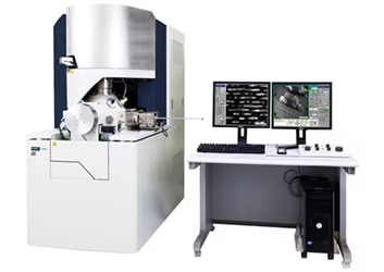
Focused Ion Beam System MI4050
The MI4050 High-Performance Focused Ion Beam System is equipped with new optics and provides the world-leading SIM imaging resolution and high-definition TEM sample preparation with improved imaging resolution at low kV. The MI4050 accommodates a variety of applications such as cross-section observation, circuit modification, vector scan processing, nano-micro patterning, nano molding, and 3D nano fabrication using deposition function.
Features
1. Greatly Reduced Processing Time Using the Big Probe Current (Maximum probe current 90 nA)
Cross-sectional processing of wire bonding (Processing size: W: 95 µm, D: 55 µm; Machining time: 20 min)
2. Ultra-Low Damaged TEM Sample Preparation by Low-kV Processing (0.5 kV or higher) and improved Secondary Electron Image Resolution at Low kV
* Less than 1kV is optional
3. High-Resolution SIM imaging (secondary electron image resolution 4 nm at 30 kV)
Cross-section SIM image of aluminium can
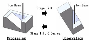
4. High-Precision 5-Axis Motorized Mechanical Eucentric Stage
The eucentric stage enables the user to specify the coordinates more accurately to obtain finer alignment for imaging and continuous processing TEM sample preparation.
5. Ease of Use and Various Processing Modes
A variety of processing modes are available with simplified operation.
- Programmed Cross Sectioning
- Programmed TEM/STEM Sample Preparation
- Continuous Auto-Pilot Processing
- Automated TEM Sample Preparation (A-TEM)
- Bitmap Processing
- Vector Scan Processing
- 3D Nano Structure Processing, and more
6. SIM Image 3D Reconstruction Analysis
Using SIM cross-section images which are obtained by equally spaced cross-sectioning and observation, 3D reconstruction analysis can be performed. It can also be used to visualize 3D information of dispersed state and hole of composite particle.
7. Circuit Modification Using Multi-Gas Injection System (MGS II) (Optional)
A variety of gasses can be injected for circuit modification, wiring, passivation, insulator, enhanced etching, and more.
- Tungsten deposition gas
- Platinum deposition gas
- Insulator deposition gas
- XeF2 etching gas
- Organic etching gas
- Carbon deposition gas
8. Variety of Coordinate Linkage Function (optional)
Hitachi High-Tech Science's proprietary coordinate linkage function offers fast and accurate coordination determination.
- Linkage between Optical Microscope and SIM image Double cursor function (Japan Patent No.4634134, US Patent No. 7595488)
- Linkage of defect inspection and coordinate Linkage with partial wafer and full wafer coordinate
- Linkage with CAD navigation system
Specifications
| Sample size | Maximum 50 mm in size and 12 mm thick |
|---|---|
| Sample stage | 5-axis motorized eucentric tilting stage |
| Accelerating Voltage | 1 - 30 kV (0.5 kV - *optional) (0.5 - 1.0 kV : 0.1 kV step) (1.0 - 2.0 kV : 0.2 kV step) |
| SIM Resolution | 4 nm@30 kV |
| Maximum Probe Current | 90 nA |
| Maximum Current Density | 50 A/cm2 |
The NANOMESH grid for FIB processing alleviates redeposit effects for high quality lamella preparation.
Numerous locations for mounting lamellae allows for high precision sample preparation and material features for better analysis.
Option
- 4ch Multi-Gas Supply System II
- Continuous Auto Pilot Software
- Automated TEM Sample Preparation (A-TEM)
- Microscopic Manipulator System, etc.
* A variety of options for MI series can be chosen.
Application Data
Material Science
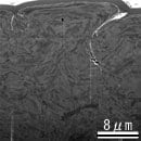
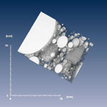
3D grain orientation analysis from serial section SIM images
Serial section SIM images
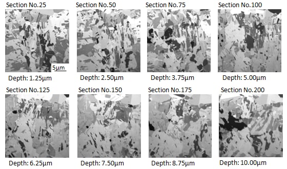
3D Reconstruction

Specimen: Copper foil
Processing Conditions
Accelerating Voltage: 30 kV
Beam Current: 12 nA
Cut size: 20 × 20 × 10 µm
Cutting interval: 50 nm
Number of cut: 200
Observation Conditions
Accelerating Voltage: 30 kV
Beam Current: 100 pA
Signal: SIM image
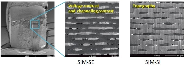
Precise distribution analysis using multiple signals
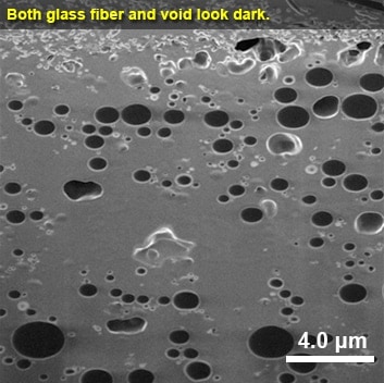
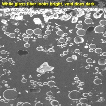
Sample: Glass epoxy resin
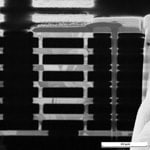
Electronics
Cross-sectional analysis with short etching
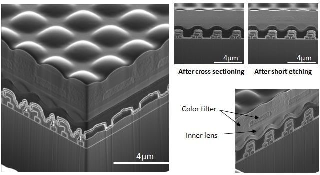
Cross-sectional analysis using multiple signals