

Ultrahigh-Resolution Schottky Scanning Electron Microscope SU8700
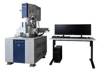
The SU8700 brings in a new era of Ultrahigh-Resolution Schottky field emission scanning electron microscopes to the long-standing Hitachi EM lineup. This revolutionary FE-SEM platform incorporates multifaceted imaging, high probe current, automation, efficient workflows for users of all experience levels, and more.
* The device photograph shows configuration with optional items.
Features
-
Hitachi’s Schottky emitter provides Ultrahigh-Resolution images and ultrafast microanalysis with high probe current.
Its 10 V* imaging capability without stage bias expands the application range for beam-sensitive specimens.
A multitude of detectors and options are available to best suit the needs of any user.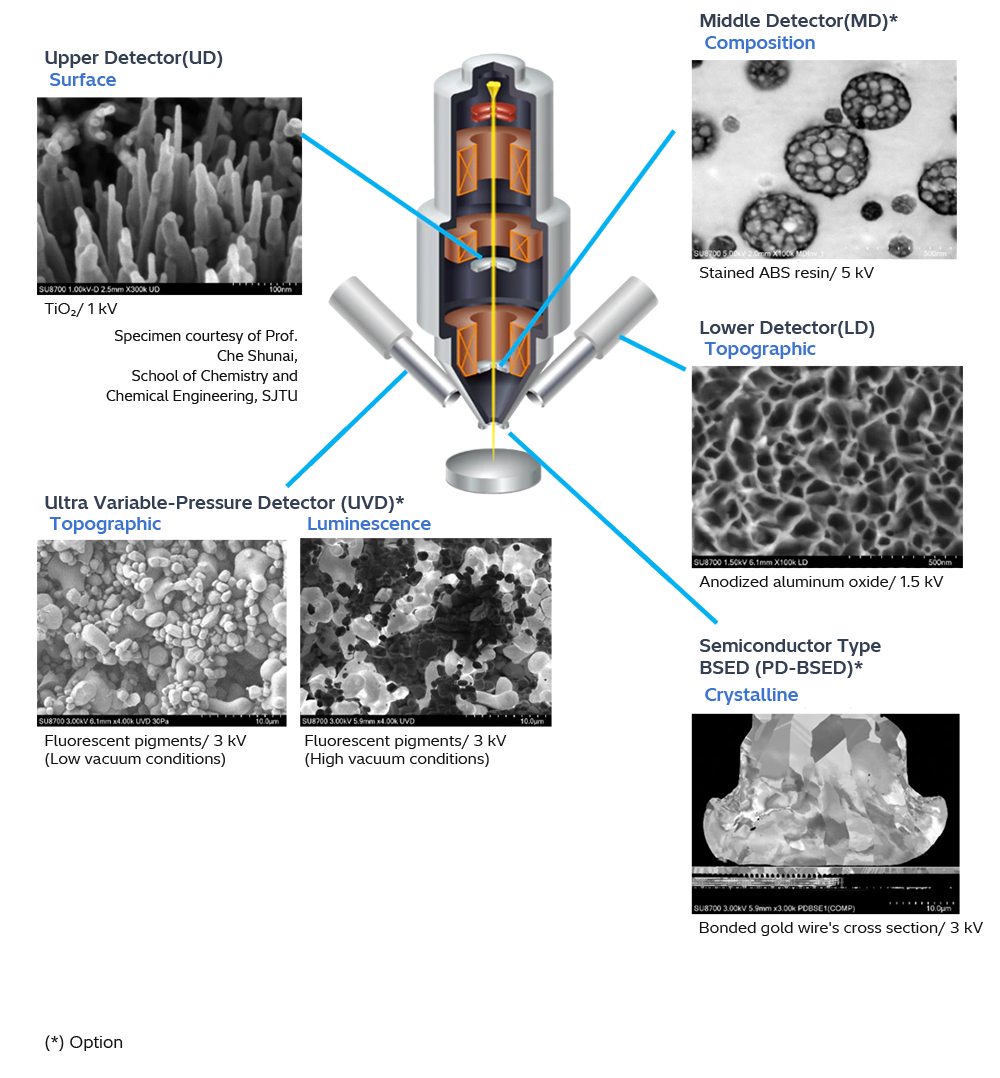
-
The “EM Flow Creator“ software option allows users to configure repeatable SEM operation sequences.
Various SEM functions can be assembled in the EM Flow Creator’s window by a drag-and-drop method and then saved as a recipe for later use.
Once a recipe is configured, automated data collection under the set conditions can be performed with high accuracy and repeatability.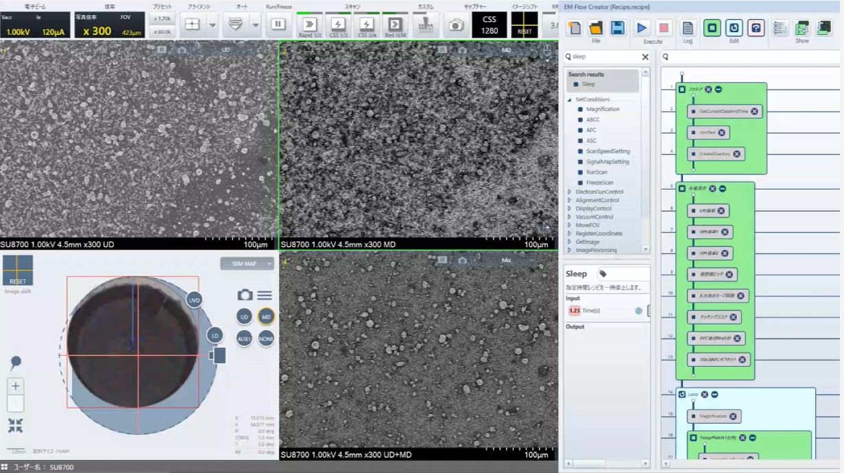
-
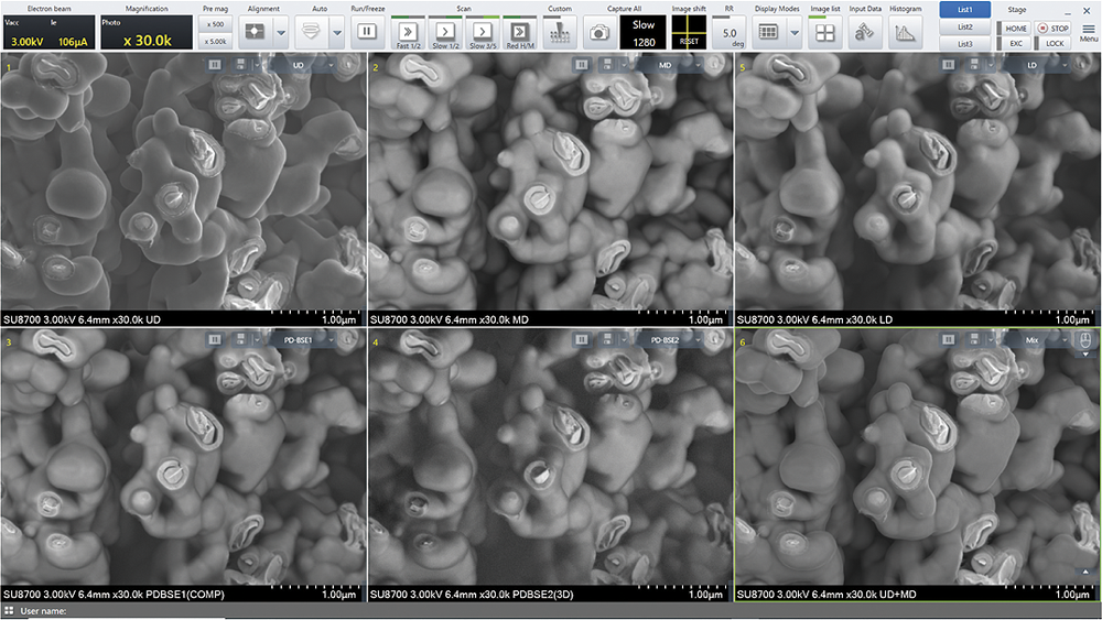
Dual monitors with 6-signal simultaneous display
1, 2, 4 or 6 signals, including the chamber scope(*) or SEM MAP, can be displayed simultaneously on a single monitor. By adding a second screen, the dual-monitor configuration supports enhanced productivity plus expanded workspace and allows the operation panel to be customized with submenus positioned anywhere on either screen.
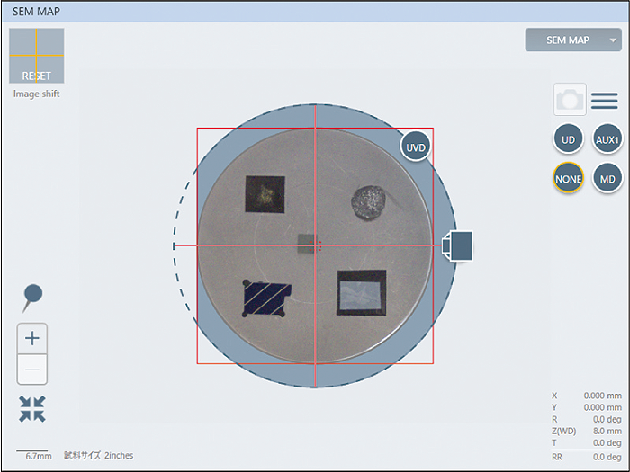
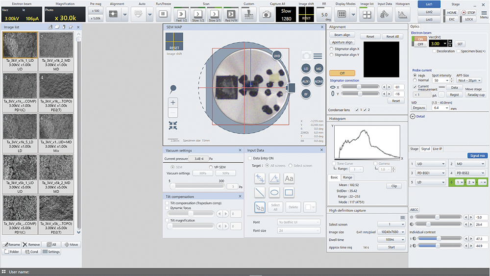 The built-in optical camera captures the specimen holder overview which is automatically transferred to the SEM MAP screen for a graphical navigation interface to assist with quick access ROI navigation.
Camera Navigation*
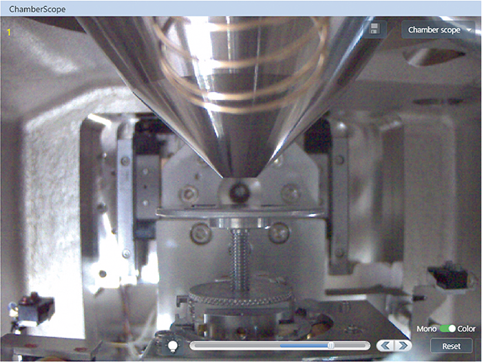
 GUI integrated chamber scope provides safe operation by showing the specimen position in real-time. This display is monochrome/color convertible and can be displayed in its own individual window.
Chamber Scope*
Chamber and Port Layout
The specimen exchange chamber accepts large specimens up to Φ150 mm diameter. Multiple EDS ports in the improved chamber design offer versatile analytical platform. (The instrument pictures includes options)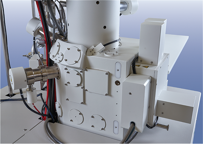
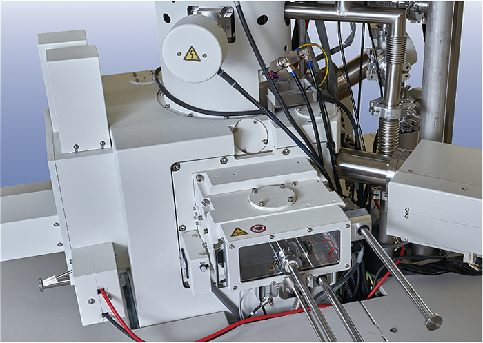
*Option
Application Data
Semiconductor
Voltage Contrast Images of 7 nm process SRAM
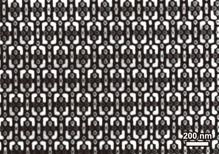
Voltage contrast in a SEM is a very powerful tool for semiconductor device evaluation. As the device structure changes by layer, SEM conditions such as accelerating voltage and contrast must also be optimized.
The SU8700 offers a voltage range down to 0.01 kV*, without stage bias, to address these needs and more. On the left is an image taken at 300 V to demonstrate this VC capability as applied to the analysis of device architecture.
Planview Image of 3D NAND Flash Memory
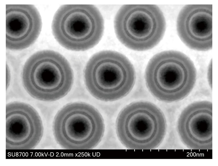
The image on the shows analysis of memory cell structure for 3D NAND.
This data clearly shows structure consisting of very thin (<10 nm) nitride, oxide and poly-Si layers. The high detection efficiency of the SU8700 allows for precise analysis of such features which are crucial to understanding capacitor structure.
*Option
Material Science
Tempered Martensite in Steel
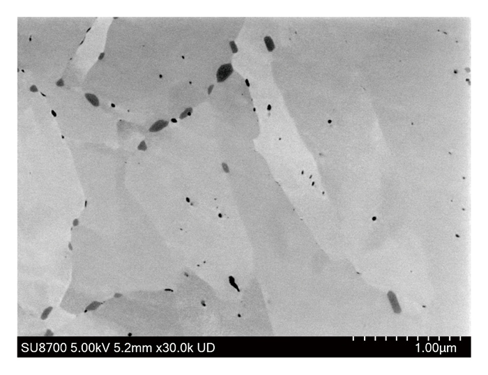
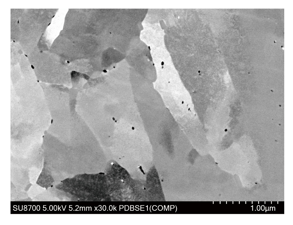
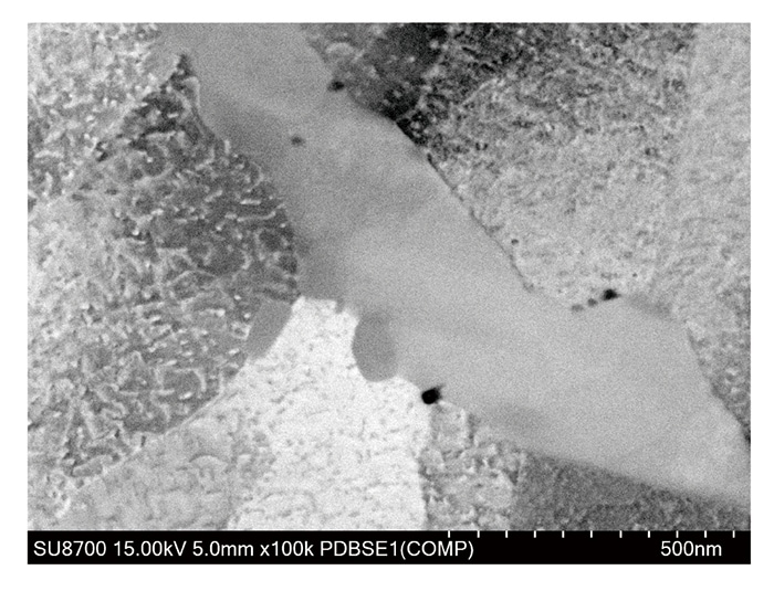
Detailed evaluation of metallic alloys is very important to many industries. The left two images demonstrate the strong capabilities of the SU8700 for such investigations.
The precipitates along grain boundaries are clearly visible when acquiring secondary electron images using the UD. Grain size and deformation are easily distinguishable in left-bottom image by acquiring BSE channeling contrast. In addition, crystal defects in some grains can be clearly observed in right-bottom image by using the same method.
Specimen courtesy of Dr. Shoichi Nambu, The University of Tokyo
Nanoparticles Containing Core-Shell Structure
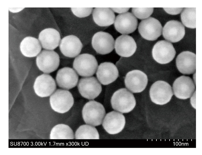
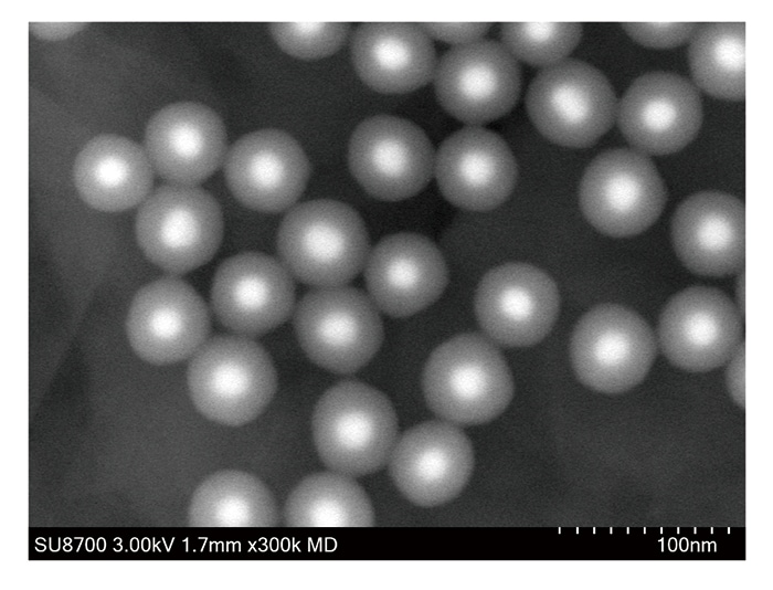
Many modern nanoparticles contain a core-shell design that is vital to their functionality.
It is essential to measure size of both the core and the shell in morphological evaluation as well as functional characterization.
In the left image above, fine surface structure is visible by SE signal (UD). In the Right image, Core (Ag) and Shell (SiO2) are easily distinguishable by BSE signal (MD).
Life Science
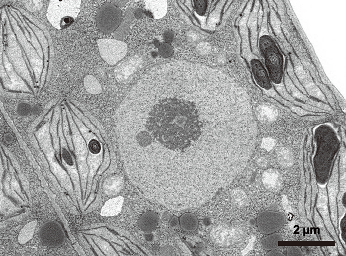
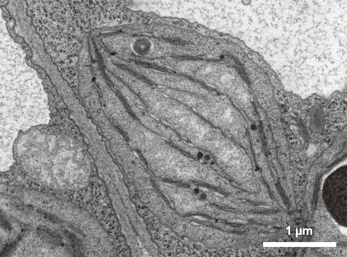
Ultrastructure of Arabidopsis thaliana
Specimen courtesy of Dr. Kiminori Toyooka, RIKEN CSRS
Backscattered electron images above from ultrathin section of Arabidopsis thaliana. Images were acquired at 2 kV of acceleration voltage to demonstrate TEM-like quality. For Energy Filtered BSE detection, ultrastructure such as thylakoid membrane are clearly visible in right image.
Large FOV + High Pixel Resolution of Rat Cerebral Cortex
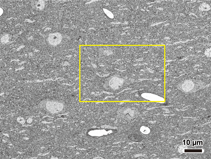
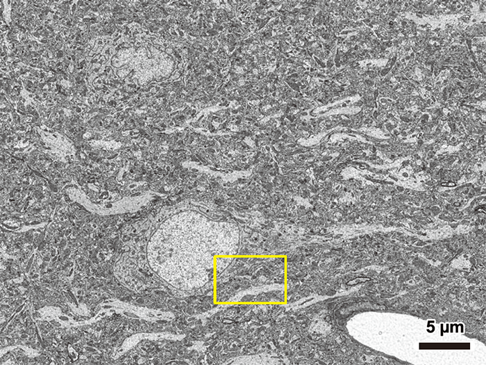
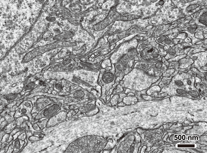
Three backscattered electron images from ultrathin section of rat forebrain demonstrate SU8700 image acquisition capability.
Top-left image was acquired with >120 µm of FOV. The yellow rectangle field in the image is also shown in bottom-left image with an increase of digital magnification. Right-bottom image is further digitally magnified and cropped from bottom-left image. Even though digitally enhanced the original image more than 20 times, the structures of organelle are clearly visible and high-quality is maintained.
High pixel resolution image up to 40,960 x 30,720 pixel available (*) on SU8700.
Specimen courtesy of Dr. Yoshiyuki Kubota,
Section of Electron Microscopy,
National Institute for Physiological Sciences
*Option
Specifications
| Electron Optics | Secondary Electron Image resolution | 0.6 nm@15 kV |
|---|---|---|
| 0.8 nm@1 kV | ||
| 0.9 nm@0.3 kV | ||
| Magnification | 20 to 2,000,000 x | |
| Electron Gun | Schottky Emitter | |
| Accelerating Voltage | 0.1 to 30 kV 0.01 to 30 kV(*3) |
|
| Landing Voltage(*1)(*3) | 0.01 to 7 kV | |
| Probe Current | Max. 200 nA | |
| Detectors | Standard Detectors | Upper Detector (UD) |
| Lower Detector (LD) | ||
| Option Detectors | Middle Detector (MD) | |
| Semiconductor Type BSED (PD-BSED) | ||
| Ultra Variable-Pressure Detector (UVD) | ||
| STEM Detector | ||
| Optional Accessories(*2) | Energy Dispersive X-ray Spectrometer (EDS) | |
| Electron Backscattered Diffraction Detector (EBSD) | ||
| Variable Pressure mode(*3) | Vacuum Range | 5 to 300 Pa |
| Specimen Stage | Stage Control | 5-axis Motor Drive |
| Movable Range | ||
| X | 0 to 110 mm | |
| Y | 0 to 110 mm | |
| Z | 1.5 to 40 mm | |
| T | -5 to 70° | |
| R | 360° | |
| Specimen Chamber | Specimen Size | Max. φ150 mm(*4) |
(*1) with deceleration mode
(*2) Mountable Detectors
(*3) Option
(*4) please contact for information on larger sizes