
Ultrahigh-Resolution Scanning Electron Microscope SU8600
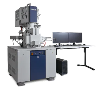
The SU8600 brings in a new era of Ultrahigh-Resolution cold-field emission scanning electron microscopes to the long-standing Hitachi EM lineup. This revolutionary CFE-SEM platform incorporates multifaceted imaging, automation, increased system stability, efficient workflows for users of all experience levels, and more.
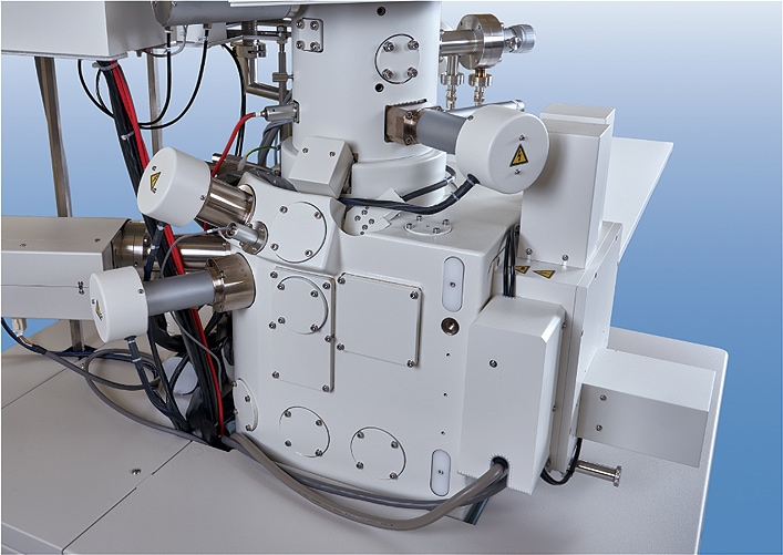
* The device photograph shows configuration with optional items.
Features
-
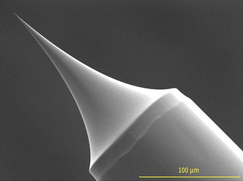
Core Technology (Cold FE Electron Source)
From the time that the cold field emission (CFE) electron source was realized in 1972, Hitachi High Tech has constantly improved this outstanding technology for high-resolution electron imaging. The latest developments in electron gun designs yield higher irradiation stability of the electron beam within the high-brightness region. The SU8600 enables high S/N imaging even at low accelerating voltages, and can also be used in long-term measurements and analyses under large current irradiation conditions rivaling other gun technologies available.
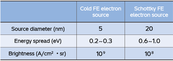
Comparison chart of electron sources for SEM
Core Technology (ExB)
Efficient detection of secondary electrons (SE) without changing the trajectory of the primary electrons is possible by forming a mutually orthogonal electric field and magnetic field (ExB field) above the objective lens. This core technology makes it possible to obtain images with excellent S/N and contrast, even at the smallest probe current conditions often used for high-resolution imaging.
Influence of electric and magnetic fields on primary electrons
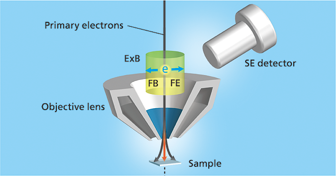
Primary electron beams pass through the ExB region without axial deviation because the actions of the electric field (E) and the magnetic field (B) are mutually cancelling.
Influence of electric and magnetic field on secondary electrons
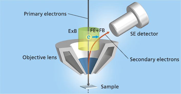
Efficient detection of SE is possible because the electric field and magnetic field act in the same direction for SEs traveling in the opposite direction to the primary electrons, forcefully directing the trajectory of the SE signal toward the SE detector.
Core Technology (SuperExB)
The advancement in design to enact SuperExB signal mixing function is one of the signature technologies of Hitachi High- Tech. The electrons (secondary electrons, SEs, or backscattered electrons, BSEs) that arrive at the SE detector are precisely controlled by changing the voltage of the signal conversion electrode in the objective lens. Simultaneous acquisition of mixed SE/BSE images can be acquired with refined selectivity.
SE mode
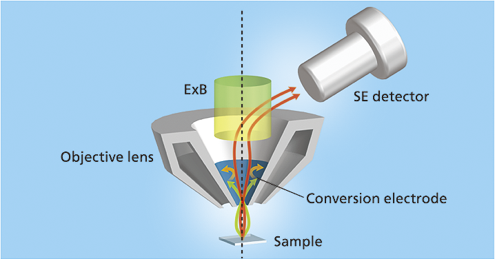
BSEs are trapped by the signal conversion electrode, and only the SEs emitted by the sample are detected.
LA-BSE mode
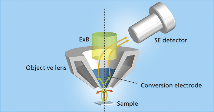
The detection rate of SEs emitted from the sample is controlled by the voltage of the signal conversion electrode. BSEs collide onto the conversion electrode, and thus resulting SEs are detected.
-
- High brightness CFE with improved stability for superb imaging.
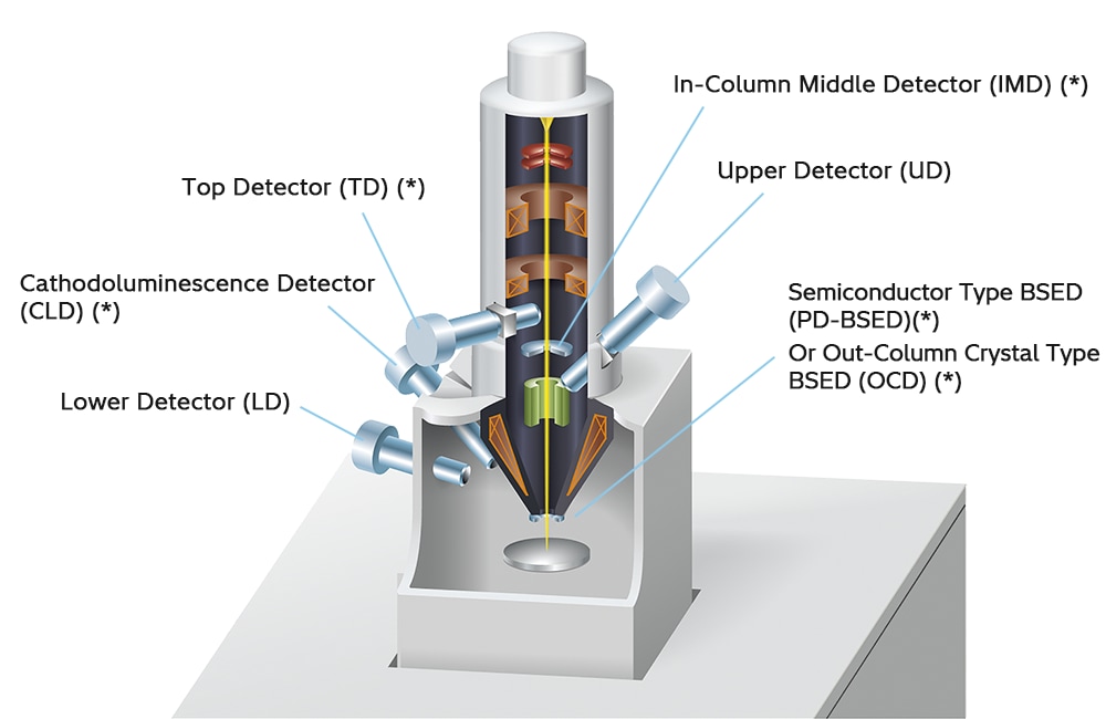
- New optional detectors (IMD, CLD, PD-BSED, OCD) for enhancing your informational experience.
*Option
Ultrahigh-Resolution
Hitachi’s high-brightness cold field emission source provides Ultrahigh-Resolution images even at Ultra-low voltages.
Specimen courtesy of Dr. Yoshihiro Kamimura,
National Institute of Advanced Industrial Science and
Technology (AIST), JapanLeft: RHO-type Zeolite particle at low-kV. In order to reveal fine steps structure on surface, the image was acquired at 0.8 kV of landing voltage. This allows the very fine structure of surface steps to be clearly visible (image on right).
A Smart Detection System for Low Voltage BSE Imaging
Cross section image of 3D NAND;
Oxide layer and Nitride layer of capacitor are easily distinguishable in the image due to BSE detection capability.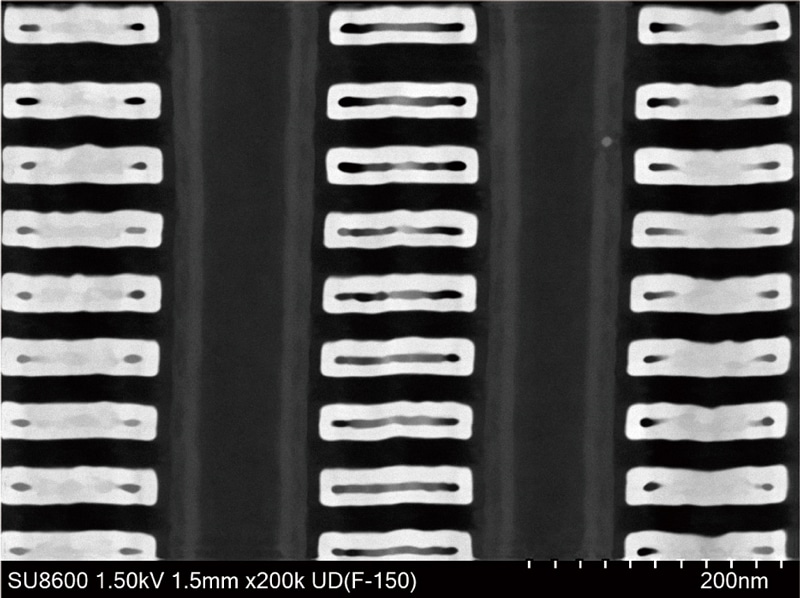
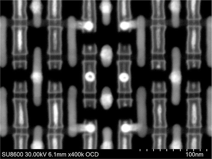
Cross Section of 3D NAND (Acceleration Voltage: 1.5 kV) Fast BSE Imaging : New Out-Column Crystal Type BSED (OCD)
By using new Out-Column Crystal Type BSED (OCD), image acquisition time was less than ONE SECOND, yet lower layer interconnect and Fin FET structure of SRAM are clearly visible.
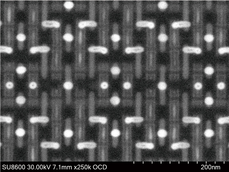
Lower Layer Interconnect of 5 nm process SRAM (Acceleration Voltage:
30 kV, Acquisition time <1 second) -
Enhanced User Experience with Advanced Automation
The “EM Flow Creator“ software option allows users to configure repeatable SEM operation sequences.
Various SEM functions can be assembled in the EM Flow Creator’s window by a drag-and-drop method and then saved as a recipe for later use.
Once a recipe is configured, automated data collection under the set conditions can be performed with high accuracy and repeatability.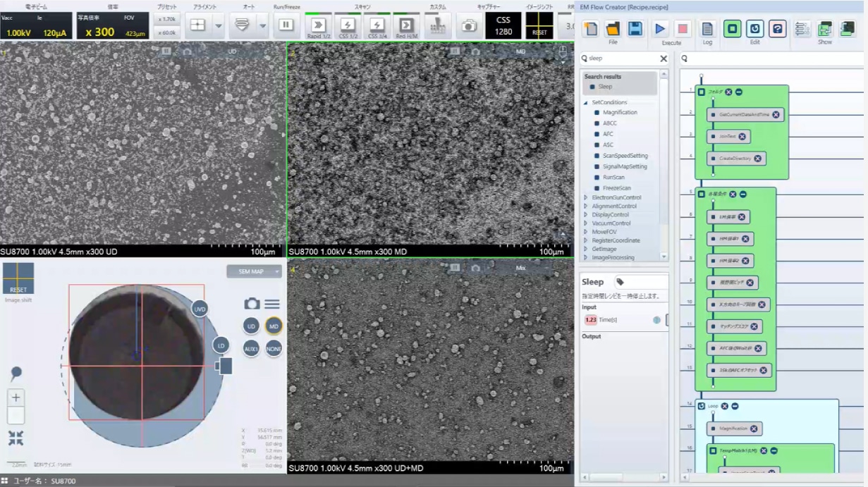
-
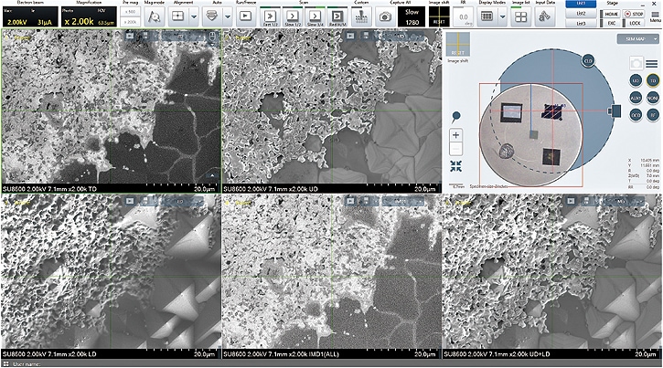
Dual monitors with 6-signal simultaneous display
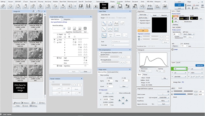
1, 2, 4 or 6 signals, including the chamber scope(*) or SEM MAP, can be displayed simultaneously on a single monitor. By adding a second screen, the dual-monitor configuration supports enhanced productivity plus expanded workspace and allows the operation panel to be customized with submenus positioned anywhere on either screen.
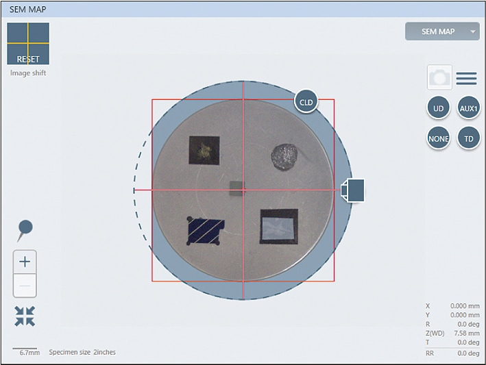
Camera Navigation*
The built-in optical camera captures the specimen holder overview which is automatically transferred to the SEM MAP screen for a graphical navigation interface to assist with quick access ROI navigation.
*Option
Chamber Scope*
GUI integrated chamber scope provides safe operation by showing the specimen position in real-time. This display is monochrome/color convertible and can be displayed in its own individual window.
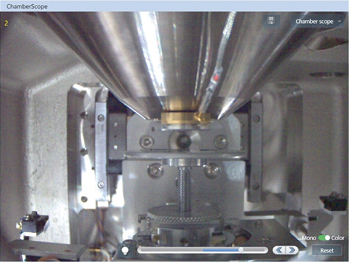
*Option
Chamber and Port Layout
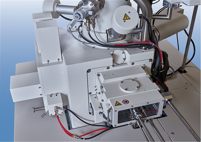
The specimen exchange chamber accepts large specimens up to Φ150mm diameter. Multiple EDS ports in the improved chamber design offer versatile analytical platform. (The instrument pictures includes options)
Application Data
Semiconductor
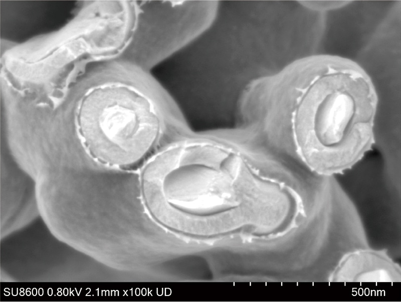
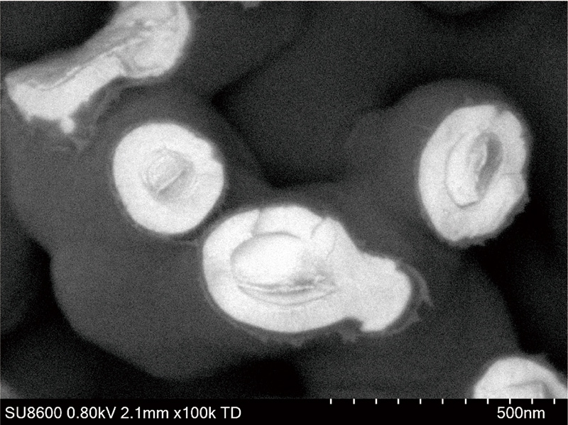
Voltage Contrast Images of 5 nm process SRAM
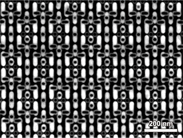
Above Left: W contact Layer, acquired at 0.5 kV (UD), Above Right: Co-W contact layer, acquired at 0.3 kV (TD) with deceleration condition. Various conditions such as landing energy, detector signal, etc. can be leveraged to effectively acquire targeted information from specific specimens.
Lower Layer Interconnect of 5 nm process SRAM
Left: Lower layer interconnect and Fin FET are visible. By using new Out-Column Crystal Type BSED (OCD), image acquisition time was less than ONE SECOND, yet structure is clearly visible. Right: Higher magnification image of ROI, demonstrating an outstanding signal to noise ration.
Cross Section Images of 3D NAND
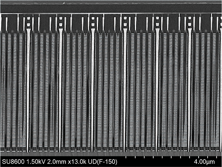
Left: Overview of cross-section image of 3D NAND. Right: Magnified image of ROI on left. Oxide layer and Nitride layer of capacitor are easily distinguishable in right image due to BSE detection capability.
Material Science
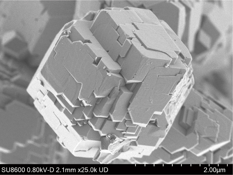
Fine Surface Structure of RHO-type Zeolite
Specimen courtesy of Dr. Yoshihiro Kamimura,
National Institute of Advanced Industrial Science and
Technology (AIST), Japan
Left: RHO-type Zeolite particle at low-kV. In order to reveal fine steps structure on surface, the image was acquired at 0.8 kV of landing voltage. This allows the very fine structure of surface steps to be clearly visible (image on right).
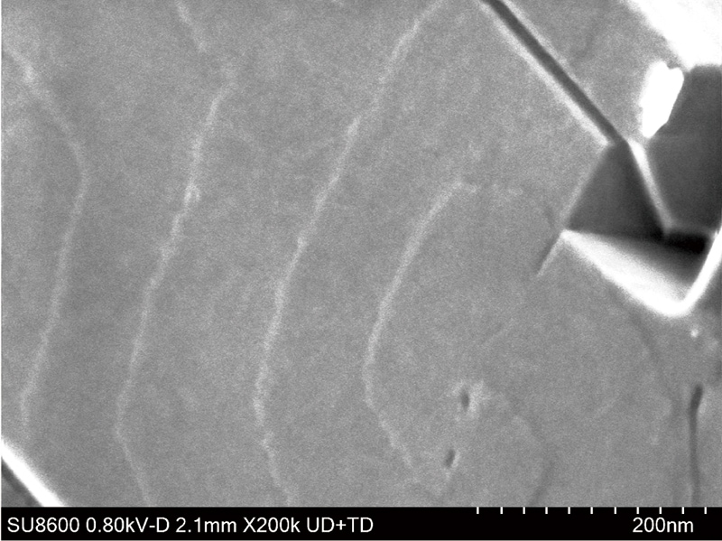
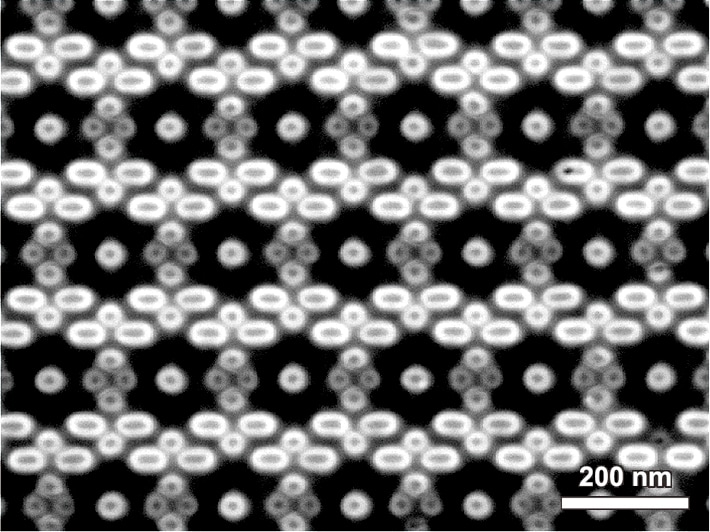
Self-Assembling Magnetic Iron Oxide Nanoparticles
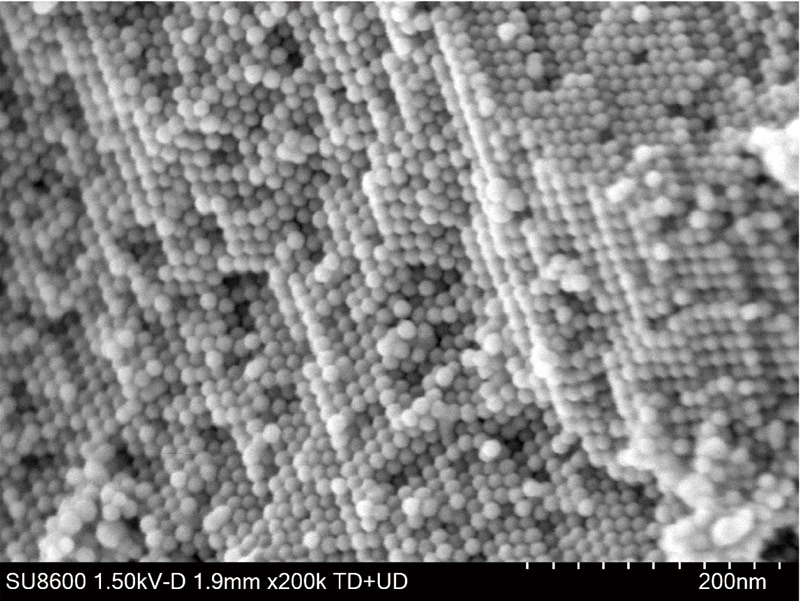
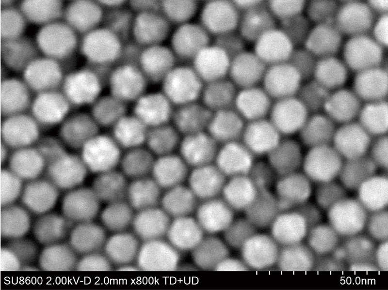
Specimen courtesy of Electrical Computer Engineering department, National University of Singapore
Left: Nanoparticles arranged in self-assembling regular sequence.
Fine structure of particles, Approx. 12 nm diameter, are visible in right image at 800 kX of magnification.
Surface Detail & Internal Composition of Capacitor Material
Surface morphology and compositional information of coated Tantalum which are used for capacitors. Simultaneous multi-signal acquisition increases sample information while reducing overall time input.
Life Science
Ultrastructure of Arabidopsis
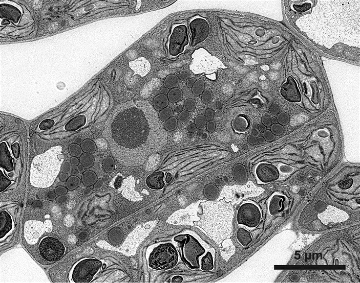
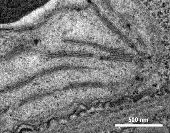
Specimen courtesy of Dr. Kiminori Toyooka, RIKEN CSR
Backscattered electron images above from ultrathin section of Arabidopsis thaliana.
Images were acquired at 2 kV of acceleration voltage to demonstrate TEM-like quality. For Energy Filtered BSE detection, ultrastructure such as thylakoid membrane are clearly visible in right image.
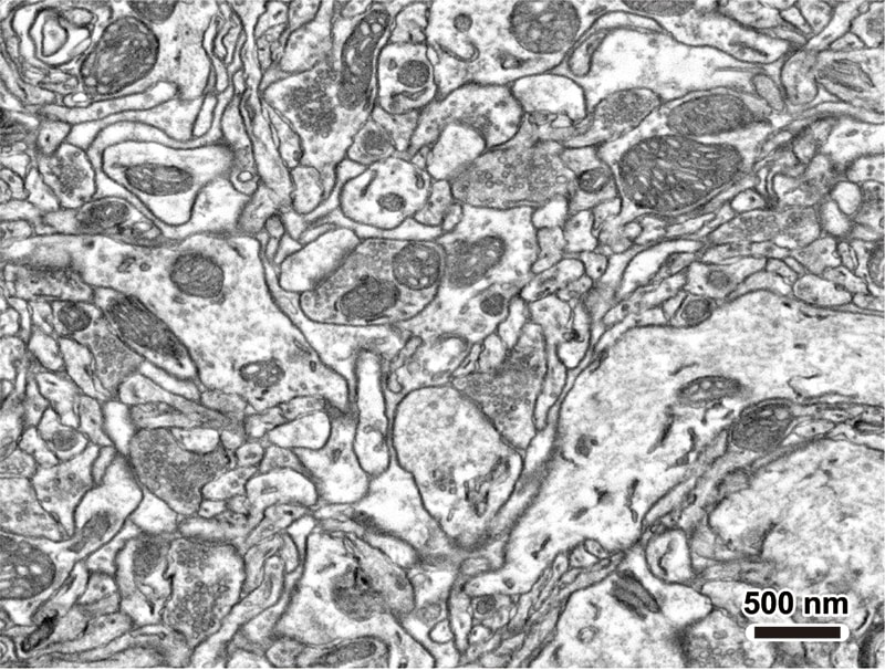
Large FOV + High Pixel Resolution of Rat Cerebral Cortex
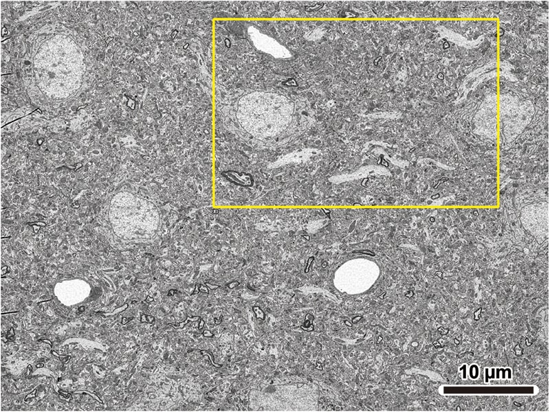
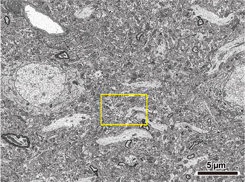
Three backscattered electron images from ultrathin section of rat cerebral cortex demonstrate SU8600 image acquisition capability.
Top-left image was acquired with >60 μm of FOV. The yellow rectangle field in the image is also shown in bottom-left image with an increase of digital magnification. Right-bottom image is further digitally magnified and cropped from bottom-left image. Even though digitally enhanced the original image more than 12 times, and high-quality is maintained.
High pixel resolution image up to 40,960 x 30,720 pixel available (*) on SU8600.
Specimen courtesy of Dr. Yoshiyuki Kubota,
Section of Electron Microscopy,
National Institute for Physiological Sciences
* Option
Specifications
| Electron Optics | Secondary Electron Image resolution | 0.6 nm@15 kV |
|---|---|---|
| 0.7 nm@1 kV (*1) | ||
| Magnification | 20 to 2,000,000 x | |
| Electron Gun | Cold cathode field emission gun with anode heating system | |
| Accelerating Voltage | 0.5 to 30 kV | |
| Landing Voltage(*1) | 0.01 to 20 kV | |
| Standard Detectors | Standard Detectors | Upper Detector (UD) with ExB filter: SE/BSE signal mixing function |
| Lower Detector (LD) | ||
| Option Detectors | Top Detector (TD) | |
| In-Column Middle Detector (IMD) | ||
| Out-Column Crystal Type BSED (OCD) | ||
| Semiconductor Type BSED (PD-BSED) | ||
| Cathodoluminescence Detector (CLD) | ||
| STEM Detector | ||
| Optional Accessories(*2) | Energy Dispersive X-ray Spectrometer (EDS) | |
| Electron Backscattered Diffraction Detector (EBSD) | ||
| Specimen Stage | Stage Control | 5-axis Motor Drive |
| Movable Range | ||
| X | 0 to 110 mm | |
| Y | 0 to 110 mm | |
| Z | 1.5 to 40 mm | |
| T | -5 to 70° | |
| R | 360° | |
| Specimen Chamber | Specimen Size | Max. φ150 mm(*3) |
(*1) with deceleration mode
(*2) Mountable Detectors
(*3) please contact for information on larger sizes