Microscopy Solutions for Materials Science
Throughout history, materials and materials science have played a critical role in the development of the world around us. Aspects of this field impact each one of us daily in the form of everything from simple household items to handheld digital devices and more. In the development of such items, the electron microscopes have been at the core of many important contributions to the field of materials science, whereby, they provided the ability to elucidate characteristics of morphology, composition, physical properties, and even dynamic behavior of incorporated materials. Such instruments are also indispensable for product quality control and understanding the development of new materials. Hitachi High-Tech offers a diverse product line-up to address these points and more, including tabletop SEM systems for quick user-friendly operation, FE-SEM as well as TEM systems for performing high-resolution analyses, and FIB-SEM systems capable of three-dimensional volumetric analysis.
Products
Imaging & Analysis

Tabletop Microscopes TM4000PlusIII/TM4000III
The TM4000PlusIII/TM4000III is the newest addition to a lineup of microscopes that have sold over 5,800 units worldwide.
Our newest updates bring improvements to users at the forefront of R&D, quality control, and education.
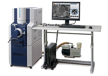
Scanning Electron Microscope FlexSEM 1000 II
The FlexSEM 1000 II VP-SEM combines innovative technological features with an intuitive interface, to deliver adaptability and flexibility in a powerful, automated, lab-friendly package. Cutting-edge technology and circuitry provides unrivaled imaging performance, even in variable-pressure environments, a feature previously only available in a full-sized SEM. This SEM runs on clean energy for an economical analytical tool, without compromising performance.
The FlexSEM will change your view of electron microscopy!
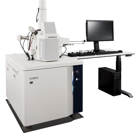
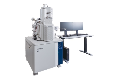
Scanning Electron Microscope SU3800/SU3900
Performance & Power in a Flexible Platform Hitachi High-Tech's scanning electron microscopes SU3800/SU3900 deliver both operability and expandability. The operator can automate many operations and efficiently utilize their high performance. The SU3900 is equipped with a large multipurpose specimen chamber to accommodate observation of large samples.
SU3900SE/SE Plus SU3800SE/SE Plus
The SU3800/3900SE Series offers high-resolution FE-SEM performance combined with user-friendly, intuitive data acquisition for a wide range of applications. With the capacity to support larger and heavier specimens than most FE-SEMs on the market, the observation of substantial specimens, such as building materials, automotive, or aerospace parts, is made possible.
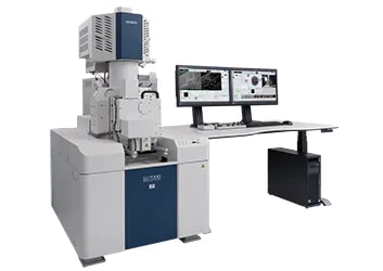
Ultrahigh-Resolution Schottky Scanning Electron Microscope SU7000
SU7000: The Next-Generation FE-SEM
The modern FE-SEM requires not only high performance but also a multitude of functionalities including wide-area observation, in-situ analysis, variable pressure, high-resolution imaging at low accelerating voltages, and simultaneous multi-signal collection.
The SU7000 is designed to address these aspects and more by delivering enhanced information for diversified needs in the field of electron microscopy.
Experience the nano-world with the SU7000!
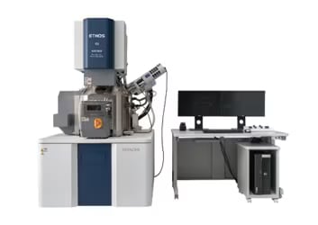
Focused Ion and Electron Beam System Ethos NX5000
Unsurpassed Performance with Ultimate Flexibility
The Hitachi Ethos FIB-SEM incorporates the latest-generation FE-SEM with superb beam brightness and stability. Ethos delivers high-resolution imaging at low voltages combined with ion optics for nanoscale precision processing.
Sample Preparation
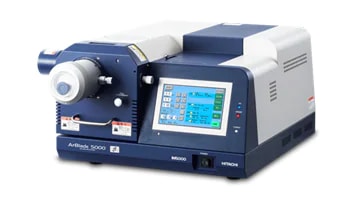
Ion Milling System ArBlade 5000
The most advanced broad ion beam system for producing exceptionally high-quality cross-section or flat-milling samples for electron microscopy.
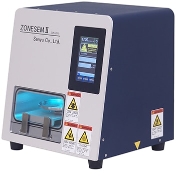
Sample Cleaner ZONESEMII
The ZONESEMⅡ。 Tabletop Sample Cleaner uses UV-based cleaning technology to minimize or eliminate hydrocarbon contamination for electron microscopy imaging.
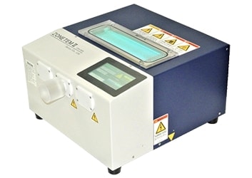
Sample Cleaner ZONETEM II
The innovative ZONETEM II Desktop Sample Cleaner uses UV-based cleaning technology to minimize or eliminate hydrocarbon contamination for electron microscopy imaging. ZONE offers easy-to-use cleaning for pre-analysis sample preparation, ensuring the best possible data from your TEM samples.
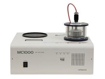
MC1000 Ion Sputter Coater
Designed and built to Hitachi’s extraordinary standards, the Hitachi MC1000 Ion Sputter Coater is poised to perform in your lab for years to come.
Related Information