
Scanning Electron Microscopes SU3800/SU3900
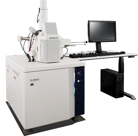
Performance & Power in a Flexible Platform
The SU3800/SU3900 scanning electron microscopes deliver power and performance through improved electron optics design. Capable of achieving high brightness even at low accelerating voltages. The microscopes are ideal for users across a variety of applications. Multiple chamber sizes are available for users to select the most effective fit for their application.
Features
-
Reliable Stage for Flexibility in Sample Size, Shape, and Weight
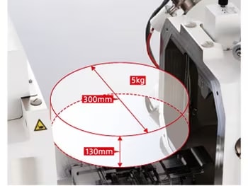
The specimen-exchange sequence helps to maintain safe operating conditions for both the sample and the SEM.
The specimen-exchange workflow displayed in the GUI guides the users through safe operation of the SEM even with large or irregular samples.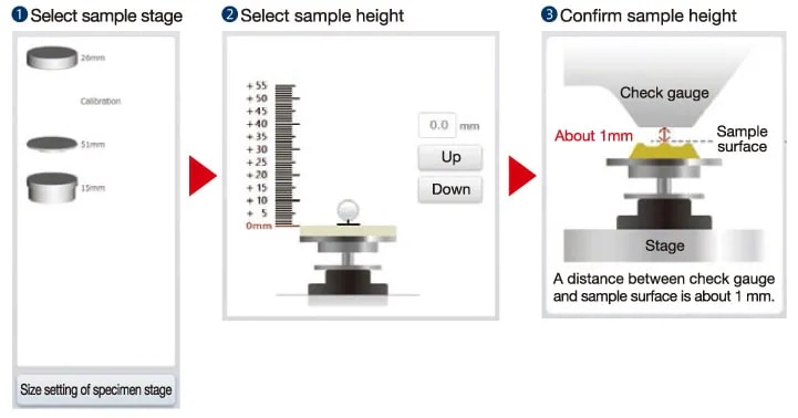
Specimen Exchange Chamber*
Exchange the specimen without venting the specimen chamber, improving throughput, vacuum cleanliness, and filament lifetime.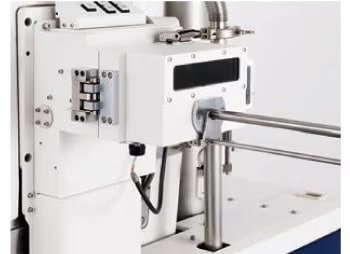
Increase sample movable range with the Stage Free Mode function*.
The microscope can be configured with Stage Free Mode*, which increases the flexibility of sample movement. This provides improved sample movement on large or irregular samples.The Chamber Scope enhances the safety of stage movements*.
The Chamber Scope is a CCD camera inside the specimen chamber and uses infrared light to monitor the system for safe sample observation. The image can be magnified to view the sample position more clearly. Utilizing the Chamber Scope allows users more confidence for safe operation.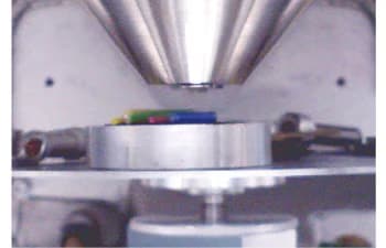
SEM MAP Expands the Boundaries of Sample Navigation*
Integrated Top-down optical camera for sample navigation
The SEM MAP camera captures wide-angle images of the sample for easy navigation. Operators can seamlessly move the sample to the area of interest by double clicking on the optical image. Users can import external images and overlay SEM images on the SEM MAP for improved imaging flexability.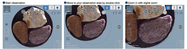
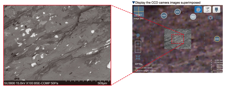
Straight-forward nagivation across the entire observable area
Wide-area SEM MAP images are obtained by automatically stitching many optical-camera images. Navigate to any location within the observable area with a single click (127 mm dia. for SU3800 and 200 mm dia. for SU3900). The stage rotates automatically during navigation as needed.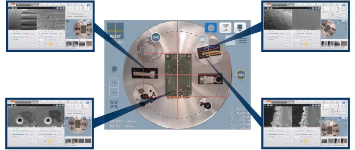
Detector-oriented rotation
The GUI makes it easy to view the orientation of the sample to the detectors. Observation of samples with topographic structures may create shadowing, causing loss of signal. Utilizing the detector-orientation information displayed in the SEM MAP allows users to quickly and accurately adjust the sample position for improved analysis.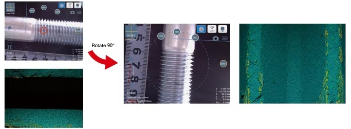
*optional
-
Multiple Modes of Operation
The SEM interface is customizable making operation flexible and easy for users of any level:
- Control stage navigation and observation conditions via mouse
- Use touchscreen and/or control panel
- Large signal display of 1280 x 960 pixels
- Simultaneous display of multiple detectors
- Standard and Advanced Display modesAutomatic Functions for Operators of Any Skill Level
Starting the accelerating voltage automatically executes AFS/ABCC/AFC/ASC for immedate specimen observation.
Automated Functions:
AFS = Filament Saturation
ABCC = Brightness Contrast Correction
AFC = Focus Correction
ASC = Stigma Correction
Auto Beam Align
Auto Optical Axis Alignment
All high-speed auto functions are improved and reduce the time to execute the function. High-quality data acquisition is faster than ever!
Improved Auto Focus function
The improved auto-focus algorithm makes it easier to quickly acquire high-quality images.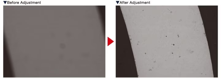
Proprietary Intelligent Filament Technology (IFT) Features:
- Automatic monitoring and control of filament condition ensures long filament life.
- Real-time monitoring and feedback displays remaining filament life.
The operator can use the SEM with confidence even for long-term continuous observation, including particle analysis.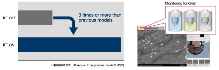
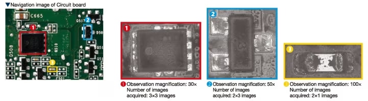
Multi Zigzag* Enables Wide-Area Observation across Multiple Areas
Hitachi's Multi Zigzag function provides automatic acquisition of large sample areas. Users define the areas of interest and the system will automatically drive to the specified locations and capture images. These images can be montaged to create a single image with high pixel resolution.
Report Creator
Report Creator allows for the export of data onto user-customizable templates. This includes SEM images, EDS maps, and camera images. Reports can be saved and edited in any Microsoft® Office format.*optional
-
20 ports for a variety of accessories
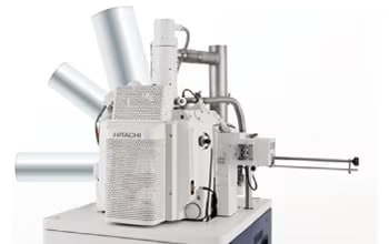
The SU3900 large chamber SEM is equipped with 20 ports to handle a variety of accessories for any application.
SEM/EDS Integration System*
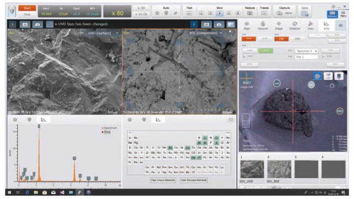
Hitachi's SEM/EDS integration system provides control and management of EDS analysis within the SEM GUI. This simplifies analysis and improves throughput by reducing unncessary switching between software and monitors.
High-Sensitivity Detectors Supporting All Observation Requirements
Cathodoluminescence (CL) Observation Using UVD*
The SU3800/SU3900 features a high-sensitivity UVD. The UVD can acquire CL and SE information. It detects light at 350-650nm, generated from collisions of secondary electrons and residual gas molecules, then accelerated by a bias electrode.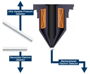
Segmented BSED allows for visualizing composition and topography
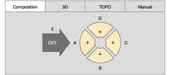
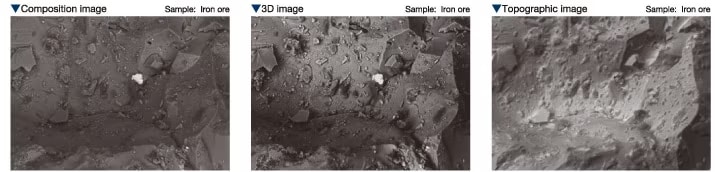
Hitachi's 5-segment BSED design is unique in that it is possible to observe composition, 3D, and topographic images from all directions without sample rotation. The design and high sensitivity of the detector allow for high-resolution imaging with improved S/N.
STEM holder*
Easily obtain transmitted images on thin samples
The newly developed STEM holder can be used to acquire transmission images in combination with Hitachi's UVD. Thinned materials and biological samples are ideal for this imaging method.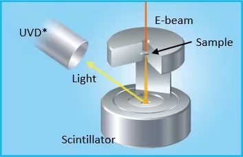
*Optional detector 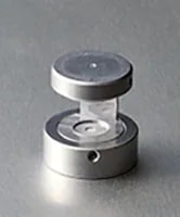
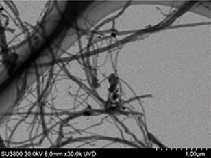
Sample : CNT
Accelerating voltage : 30 kV
Image signal : STEM
Magnification : 30,000x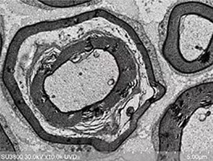
Sample : Sciatic nerve section
Accelerating voltage : 30 kV
Image signal : STEM
Magnification : 10,000x3D Modeling Software: Hitachi map 3D*
Hitachi map 3D utilizes the BSED to automatically capture 4 images from each annular segment to generate a 3D model.
- Images are captured simultaneously
- No need for sample tilting or FOV matching
- Obtain height, surface roughness, line roughness, and more.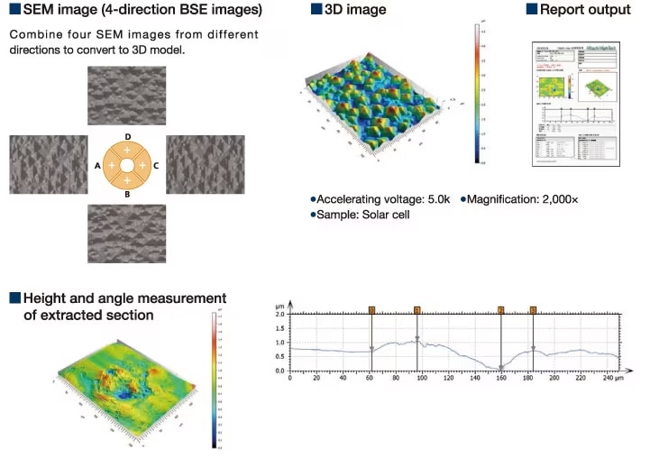
Image Processing, Measurement, and Analysis Software: Image-Pro® for Hitachi*2
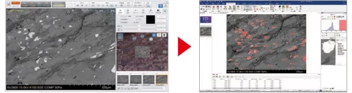
The SU3800/SU3900 features Image-Pro Transfer (IPI). IPI automatically transfers SEM images to Image-Pro® for automated image analyses resulting in immediate feedback.
*optional
*2(Image-Pro® manufactured by Media Cybernetics Inc.)
Technical Explanation
Specification
| Items | Product Features | ||
|---|---|---|---|
| SU3800 | SU3900 | ||
| Secondary Electron Resolution | 3.0 nm (accelerating voltage 30 kV, WD=5 mm, high vacuum mode) | ||
| 15.0 nm (accelerating voltage 1 kV, WD=5 mm, high vacuum mode) | |||
| Backscattered Electron Resolution | 4.0 nm (accelerating voltage 30 kV, WD=5 mm, low vacuum mode) | ||
| Magnification | ×5 to ×300,000 (magnification of image*1) | ||
| ×7 to ×800,000 (magnification of actual display*2) | |||
| Accelerating Voltage | 0.3 kV to 30 kV | ||
| Low Vacuum Mode Setting | 6 to 650 Pa | ||
| Image Shift | ± 75 µm (WD=10 mm) | ||
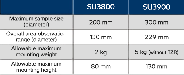
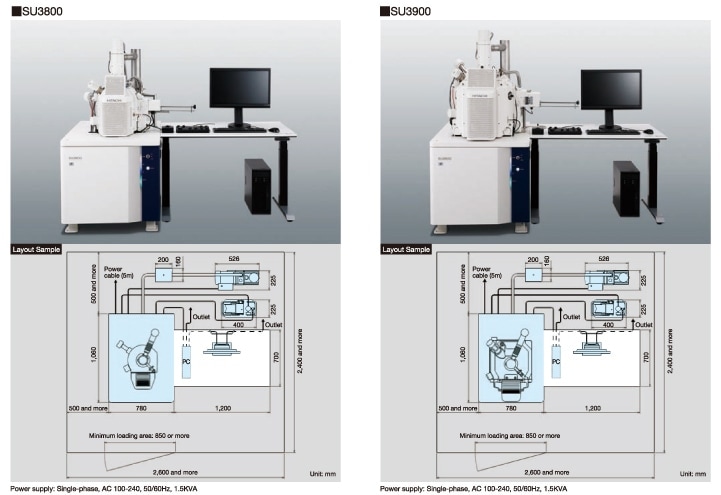
| Maximum Specimen Size | Φ 200 mm | Φ 300 mm | |
| Specimen Stage | X | 0 to 100 mm | 0 to 150 mm |
| Y | 0 to 50 mm | 0 to 150 mm | |
| Z | 5 to 65 mm | 5 to 85 mm | |
| R | 360° in continuous mode | ||
| T | -20 to +90° | ||
| Maximum Movable Range | Φ 130 mm (in combination with R) | Φ 229 mm (in combination with R) | |
| Maximum Movable Height | 80 mm (WD= 10 mm) | 130 mm (WD= 10 mm) | |
| Motor Drive | 5-axis motor drive | ||
| Electron Optics | Electron-Gun | Pre-centered cartridge type tungsten hairpin filament | |
| Objective-Lens Aperture | 4-hole movable aperture | ||
| Detectors | Secondary electron detector, sensitive semiconductor backscattered electron detector | ||
| WD for EDX analysis | WD=10 mm (T.O.A=35°) | ||
| Image Display | Auto-Axis Alignment. Function | Beam control : auto (AFS→ABA→AFC→ABCC) | |
| Optical axis adjustment: auto (current alignment) | |||
| Beam brightness: auto | |||
| Auto Image Adjustment Function | Auto brightness and contrast control (ABCC) | ||
| Auto focus control (AFC) | |||
| Auto stigma and focus (ASF) | |||
| Auto filament saturation (AFS) | |||
| Auto beam alignment (ABA) | |||
| Auto start (HV-ON→ABCC→AFC) | |||
| Operation Auxiliary Function | Raster rotation, dynamic focus, image improvement function, Data input (point-to-point measurement, angle measurement, texts),preset magnification, Stage positioning navigation function (SEM MAP), beam marking function | ||
| Optional function | ■Hardware: Track ball, Joystick, Operation panel, Compressor, Ultra sensitive low vacuum detector (UVD), Chamber scope, Camera navigation system ■Software: SEM data manager, External communication interface, 3D-capture, Stage free mode, EDS integration | ||
| Options(for External Devices) | Energy dispersive X-ray spectrometry (EDS), Electron Backscatter Diffraction(EBSD), External stage (cooling stage) |
||
*1 Set magnification with 127 mm x 95 mm (4" x 5" picture size) as display size.
*2 Set magnification with 509.8 mm x 286.7 mm (1,920 x 1,080 pixels) as display size.
Related Information