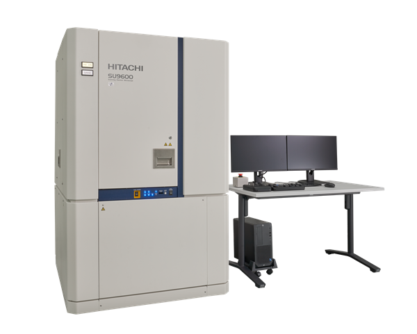
Ultrahigh-Resolution Scanning Electron Microscope SU9600
The world's highest resolution SEM
— now with higher throughput and improved automation with efficient workflows.
The SU9600: Hitachi's new Flagship Cold Field SEM
Nanometer-scale morphology observation is critical due to the trend of decreasing feature sizes in semiconductor devices and the development of advanced materials. With respect to this, Hitachi High-Tech has developed the SU9600 Scanning Electron Microscope (SEM) that enables subnanometer observations. The new SU9600 system retains the world's highest resolution* of 0.4 nm at 30 kV. It also boasts high throughput and stability making it a powerful tool for research and characterization of next-generation materials.
* As of October 2025
Key features of the SU9600
- Ultrahigh-Resolution observations enabled by Hitachi's proprietary technology
- Next-generation imaging capabilities enable highly efficient observation workflows without sacrificing resolution
- A host of new functionality to support automation and streamlined instrument operation
Core Technology
Cold field-emission electron source
Cold field-emission (FE) electron sources offer unparalleled capabilities for high-resolution observation.
Hitachi High-Tech introduced the first commercial cold FE electron source in 1972 and has worked continuously to improve the technology ever since. The SU9600 is equipped with our latest electron gun that provides stable beam irradiation and high brightness. In addition to enabling image acquisition with a high signal-to-noise ratio even at low accelerating voltages, the SU9600 allows stable observations that require high probe-current irradiation over a long period of time.
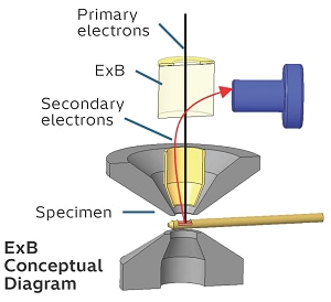
ExB
Efficient detection of secondary electrons (SE), without changing the trajectory of the primary electrons, is possible by forming a mutually orthogonal electric and magnetic field (ExB field) above the objective lens. This core technology makes it possible to obtain images with excellent S/N and contrast, even at low probe-current settings which are often required for high-resolution imaging.
Low-aberration in-lens objective lens
In-lens objective lens has the advantage of reducting spherical and chromatic aberration effectively by shortening the focal length. Compared to conventional lens designs, Hitachi's in-lens objective lens enables acquisition of higher-resolution images. It also provides stable observation of micro structures on the scale of a few nanometers or below.
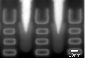
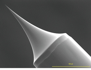
(GAA structure cross section)
Accelerating voltage: 7 kV
Magnification: 1,000 kx
Complete Lineup of Detectors
The SU9600 incorporates multiple detectors to allow acquisition of secondary-electron, backscattered-electron, and transmission-electron signals. New secondary-electron signal-control capabilities enable a wide variety of observation modes that can be optimized for any type of specimen. The newly-developed variable crystal detector (VCD), a scintillator-based backscattered-electron detector, improves response times, making it easier to pinpoint specific observation regions.
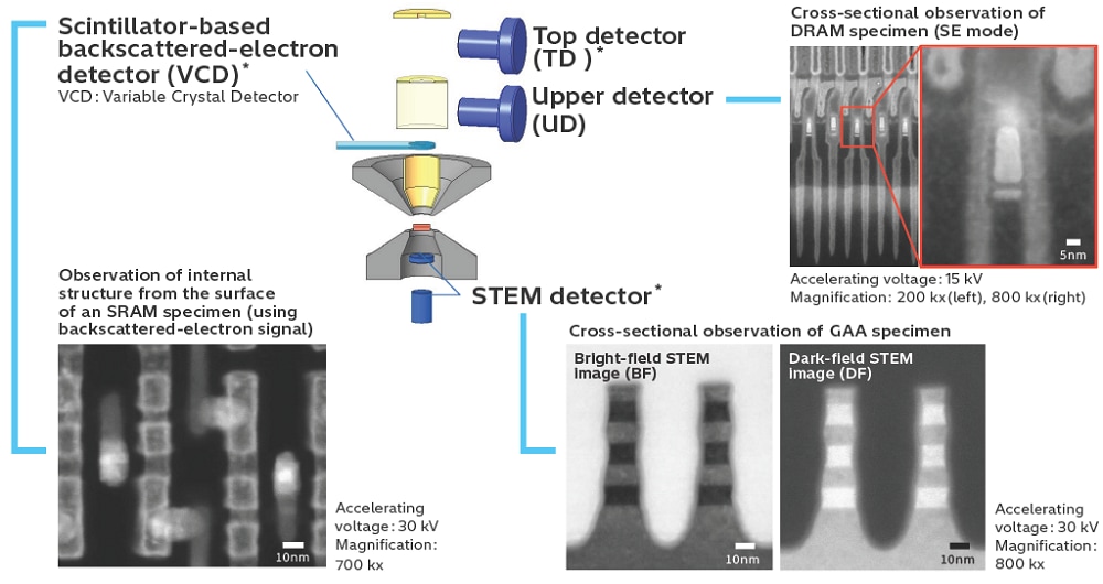
* Option
Enhanced scanning capabilities
The SU9600 provides many improved scanning capabilities to optimize image acquisition for a variety of specific purposes. This enables more efficient observation workflows—and can be combined with EM Flow Creator* to automate various scanning procedures.
[Enhanced scanning features]
- Dwell time configurable over a wide range
- Support for imaging only specific regions of interest at arbitrary locations within the field of view *
- Capture highly detailed images up to 40,960 × 30,720 pixels *
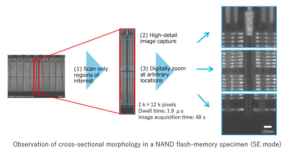
* Option
Key Specifications
| Items | Description | |
|---|---|---|
| Electron gun | Cold cathode field emission source | |
| SE image resolution | Secondary Electron Image Resolution: 0.4 nm @ 30 kV | |
| 1.0 nm @ 1 kV | ||
| 0.6 nm @ Landing Voltage of 1 kV *1 | ||
| STEM image resolution *2 | 0.34 nm @ 30 kV (lattice image) | |
| Accelerating voltage | 0.5 to 30 kV | |
| Landing voltage *1 | 0.01 to 20 kV | |
| Magnification | 80 to 3,000,000 x | |
| Maximum pixel size | 10,240 × 7,680、40,960 × 30,720*2 pixels | |
| Stage | Side entry goniometer stage | |
| Stage traverse | X: ±4.0 mm、Y: ±2.0 mm、Z: ±0.3 mm、T: ±40 ° | |
| Specimen size | Flat specimen stage | 5.0 mm × 9.5 mm × 3.5 mm (H) (Max.) |
| Cross section specimen stage | 2.0 mm × 6.5 mm × 5.0 mm (H) (Max.) | |
| Detector | Detector | Secondary electron detector (with SE/BSE signal mixing capabilities) |
| Top detector*2 | ||
| VCD (Variable Crystal Detector)*2 | ||
| BF/DF Duo-STEM detector*2 | ||
| Energy dispersive X-ray detector*2 | ||
*1: With optional deceleration holder and top detector.
*2: Option
This journal addresses a wide range variety of research papers and useful application data using Hitachi science instruments.
Related Information