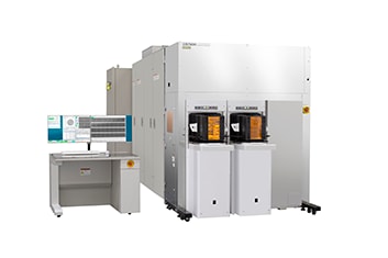
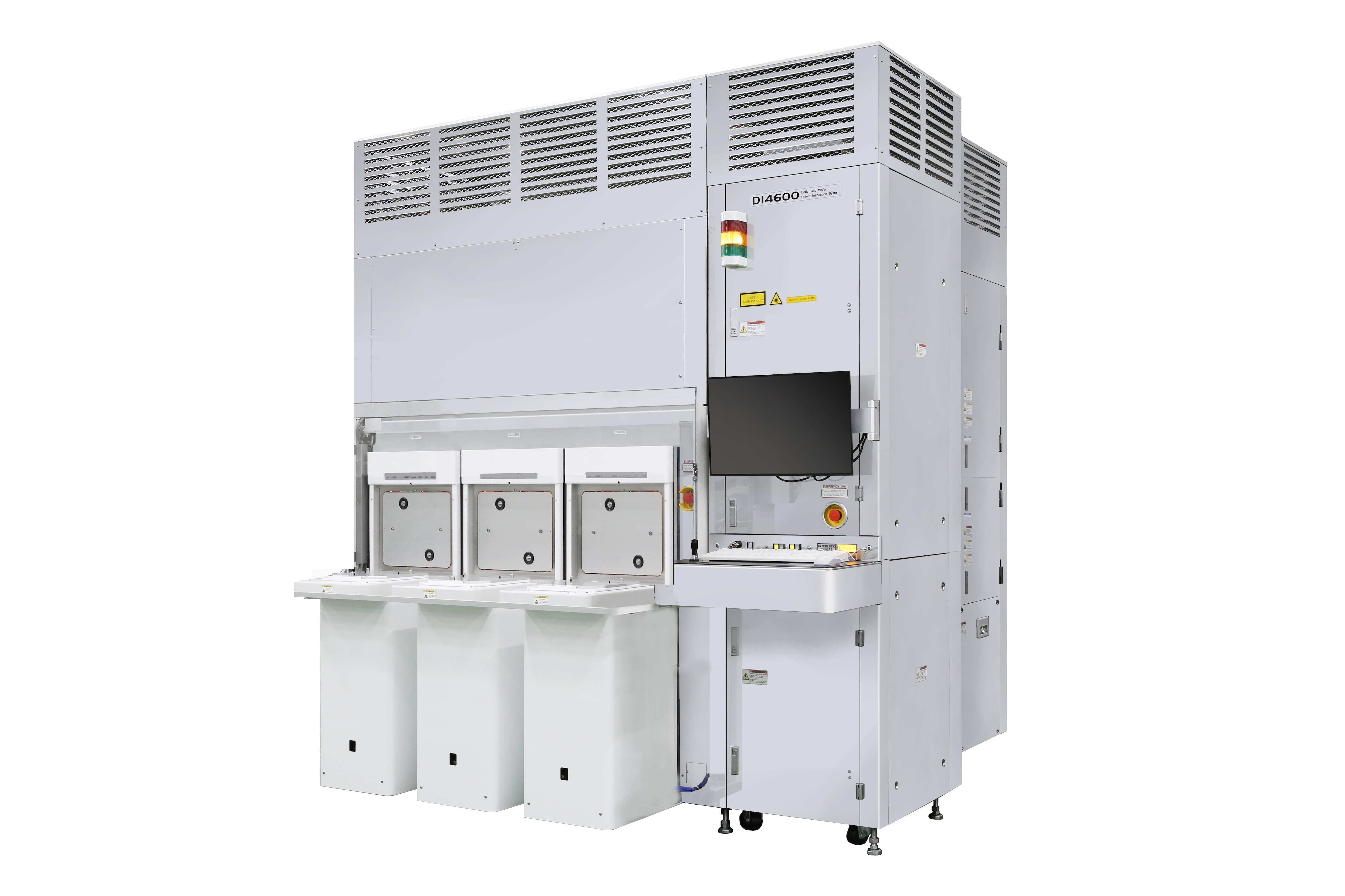
Dark Field Wafer Defect Inspection System DI4600
In the production lines of semiconductor fabs, abnormalities should be quickly detected to avoid yield loss.
To meet this need, DI4600 is designed to detect defects on patterned wafers with high sensitivity and throughput. High sensitivity and throughput are realized by the combination of the sheet-beam optics and the accurate light separation with spatial filters.
DI4600 systems are installed and running as in-line defect management tools in the cutting-edge memory and logic semiconductor fabs.
Features
Higher throughput and detection sensitivity for high-volume production
- As dark-field wafer-defect inspection systems, DI4600 contributes to manage semiconductor production lines.
Higher matching performance between tools
- DI4600 adopts an original optics designed for fleet operation.
Easy operation
- Parameters for inspection recipes are simple.
Wafer Size
- φ300mm