
Ultrahigh-Resolution Scanning Electron Microscope SU9600

The world's highest resolution SEM
— now with higher throughput and improved automation with efficient workflows.
The SU9600: Hitachi's new Flagship Cold Field SEM
Nanoscale structural analysis requires more than high-resolution imaging. It also requires optimized signal acquisition for different imaging conditions and comprehensive analysis using multiple signals.
The SU9600 combines a low-aberration in-lens objective lens with a high-brightness cold field-emission electron gun to deliver stable, high-resolution SEM imaging across a wide range of accelerating voltages. Its ExB detection system enables highly efficient signal collection for high-contrast imaging.
Simultaneous SEM/STEM imaging provides multiple types of information in a single session, including surface morphology, internal structure, and crystallographic information. By correlating these datasets, users can gain deeper insight into the condition and properties of the sample.
With these advanced imaging and analytical capabilities, the SU9600 supports precise analysis across a wide range of applications, from research and development to quality evaluation in manufacturing.
*1 Secondary electron image resolution: 0.4 nm
*2 As of October 2025
Key features of the SU9600
-
Cold field-emission electron source
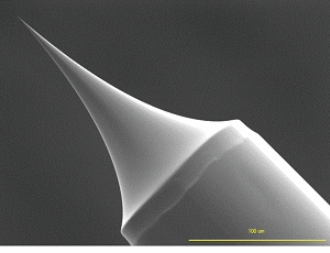
Cold field-emission (FE) electron sources offer unparalleled capabilities for high-resolution observation.
Hitachi High-Tech introduced the first commercial cold FE electron source in 1972 and has worked continuously to improve the technology ever since. The SU9600 is equipped with our latest electron gun that provides stable beam irradiation and high brightness. In addition to enabling image acquisition with a high signal-to-noise ratio even at low accelerating voltages, the SU9600 provides stable emission current for applications that require high probe-current irradiation over a long period of time.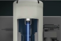
Unique Side-Entry Holder Design for In-lens System
The SU9600 combines an in-lens objective lens with a unique side-entry specimen holder design. This configuration provides a short focal length while minimizing the effects of spherical and chromatic aberrations.
Compared with conventional lens systems, this advanced optical design delivers higher-resolution images and enables stable observation of fine structures only a few nanometers or less.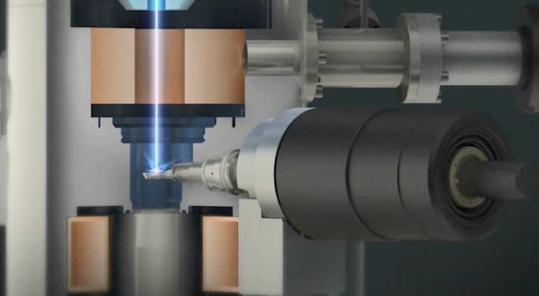
ExB Detection System for Efficient Signal Collection
Efficient detection of secondary electrons (SE), without changing the trajectory of the primary electrons, is possible by forming a mutually orthogonal electric and magnetic field (ExB field) above the objective lens. This core technology makes it possible to obtain images with excellent S/N and contrast, even at low probe-current settings which are often required for high-resolution imaging.
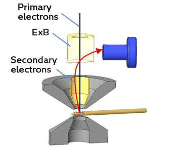
ExB Conceptual Diagram -
The SU9600 incorporates multiple detectors to allow acquisition of secondary-electron, backscattered-electron, and transmission-electron signals. New secondary-electron signal-control capabilities enable a wide variety of observation modes that can be optimized for any type of specimen. The newly-developed variable crystal detector (VCD), a scintillator-based backscattered-electron detector, improves response times, making it easier to pinpoint specific observation regions.
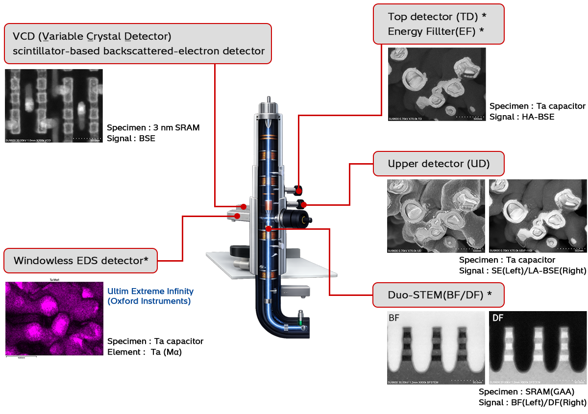
*Option
-
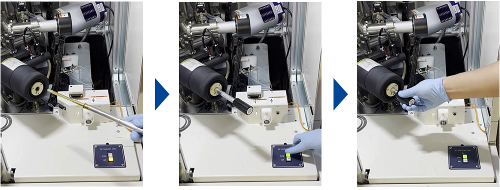
Side-Entry Holder for High-Resolution Imaging and Rapid Sample Exchange
The sample position is optimized for high-resolution imaging, while the side-entry specimen holder design enables quick and easy sample exchange.
-
Hitachi's “EM Flow Creator“ software option allows users to configure repeatable SEM operation sequences.
By automating the inspection workflow, from setting observation conditions to image acquisition, the system enables efficient and highly reproducible data collection.
The automation software allows individual operations, such as magnification setting, stage positioning, and focus and contrast adjustment, to be configured as functional blocks. By combining these blocks, users can intuitively create customized observation recipes.
Executing a configured recipe enables smooth, continuous image acquisition and large-area observation. This streamlines observation workflows and reduces operator dependency, providing powerful support for consistent and reliable data acquisition across a wide range of applications, from research and development to quality evaluation.
Number of images acquired: 56
Magnification: 250,000 x
Acquisition time: Approximately 15 minutes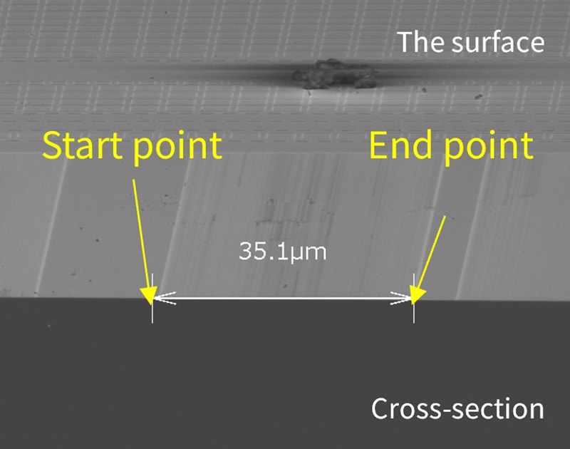
Perspective view of the cross section *Option
Application data
Semiconductors
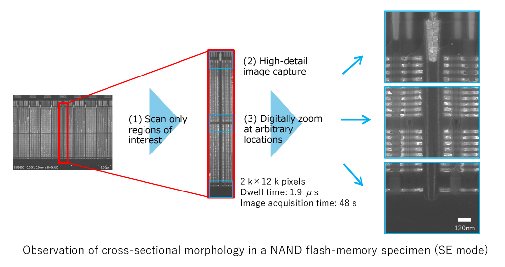
The SU9600 provides many improved scanning capabilities to optimize image acquisition for a variety of specific purposes. This enables more efficient observation workflows—and can be combined with EM Flow Creator* to automate various scanning procedures.
[Enhanced scanning features]
- Dwell time configurable over a wide range
- Support for imaging only specific regions of interest at arbitrary locations within the field of view *
- Capture highly detailed images up to 40,960 × 30,720 pixels *
* Option
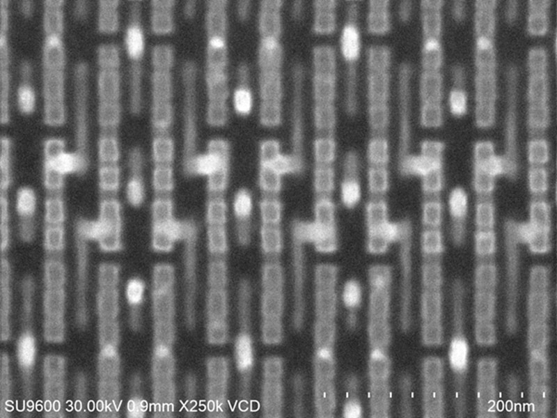
Newly Developed Fast-Response Backscattered Electron Detector: VCD (Variable Crystal Detector)*
The newly-developed variable crystal detector (VCD), a scintillator-based backscattered-electron detector provides a fast response, enabling clear backscattered electron image acquisition even with scan times of less than one second. The position of the detector can be adjusted to acquire compositional and topographic information, supporting flexible imaging for different observation purposes.
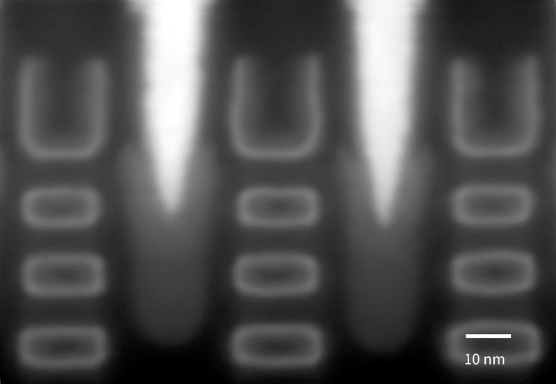
BF/DF Duo-STEM Detector for Flexible Transmitted Electron Imaging
The BF/DF Duo-STEM detector enables both bright-field and dark-field STEM imaging. In dark-field mode, users can select the range of scattering angles used for signal acquisition, allowing imaging conditions to be optimized for different observation purposes.
By adjusting the distance between the sample and the dark-field detector plane, users can also perform high-angle annular dark-field (HAADF) imaging with enhanced atomic-number (Z) contrast.
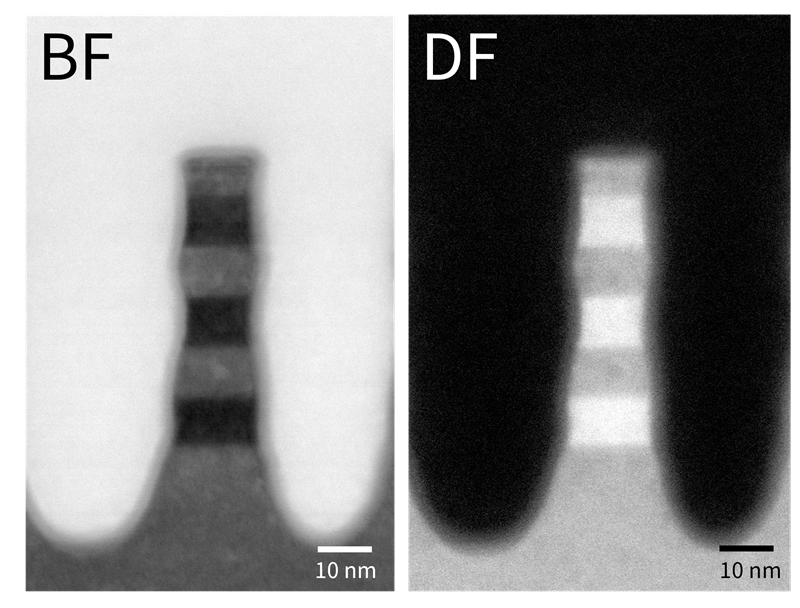
Signals: BF (Left) / DF (Right)
Magnification: 800 k
Materials Science
High-Resolution STEM and SEM Imaging with an In-Lens System
The SU9600 combines a low-aberration in-lens objective lens with an advanced electron optical system optimized for STEM, enabling high-resolution imaging in both STEM and SEM modes.
Users can easily switch between the two imaging modes to examine fine structures from different perspectives. This flexibility supports detailed and reliable characterization for a wide range of applications, including materials characterization and device analysis.
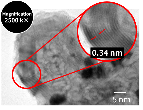
Signal: BF‑STEM
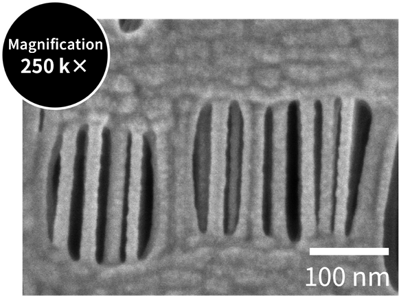
Signal: Secondary electrons (deceleration)
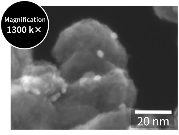
Signal: Secondary electrons
High-Contrast STEM Imaging of Light-Element Materials at Low Accelerating Voltages
Low-accelerating-voltage STEM imaging enhances the interaction between the electron beam and the sample, especially for materials composed primarily of light elements, providing improved image contrast.
This capability enables clear visualization of fine structures in materials such as organic compounds, polymers, and biological specimens, supporting detailed characterization across a wide range of applications.
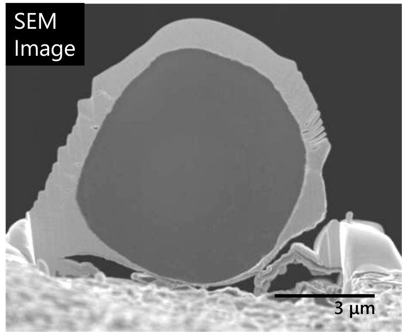
Data acquired with SU9000 II
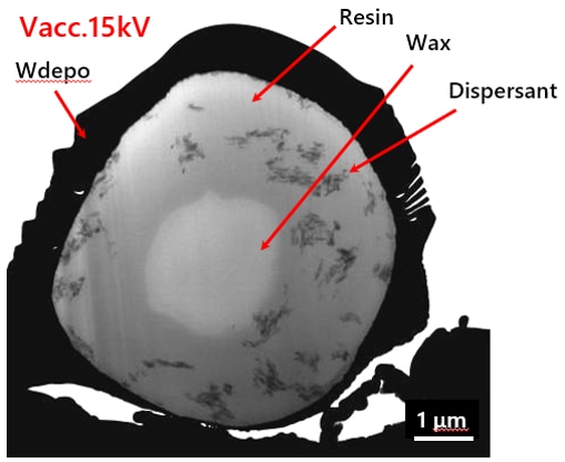
Signal: BF
Key Specifications
Specifications
| Items | Description | |
|---|---|---|
| SE image resolution | Secondary Electron Image Resolution: 0.4 nm @ 30 kV | |
| 1.0 nm @ 1 kV | ||
| 0.6 nm @ Landing Voltage of 1 kV *1 | ||
| STEM image resolution *2 | 0.34 nm @ 30 kV (lattice image) | |
| Accelerating voltage | 0.5 to 30 kV | |
| Landing voltage *1 | 0.01 to 20 kV | |
| Stage traverse | X: ±4.0 mm、Y: ±2.0 mm、Z: ±0.3 mm、T: ±40 ° | |
| Specimen size | Flat specimen stage | 5.0 mm × 9.5 mm × 3.5 mm (H) (Max.) |
| Cross section specimen stage | 2.0 mm × 6.5 mm × 5.0 mm (H) (Max.) | |
System Configuration and Features
| Items | Description | |
|---|---|---|
| Electron gun | Cold cathode field emission source | |
| Magnification | 80 to 3,000,000 x | |
| Maximum pixel size | 10,240 × 7,680、40,960 × 30,720*2 pixels | |
| Detector | Detector | Secondary electron detector (with SE/BSE signal mixing capabilities) |
| Top detector*2 | ||
| VCD (Variable Crystal Detector)*2 | ||
| BF/DF Duo-STEM detector*2 | ||
| Energy dispersive X-ray detector*2 | ||
*1: With optional deceleration holder and top detector.
*2: Option
Related Information