Metrology Solution
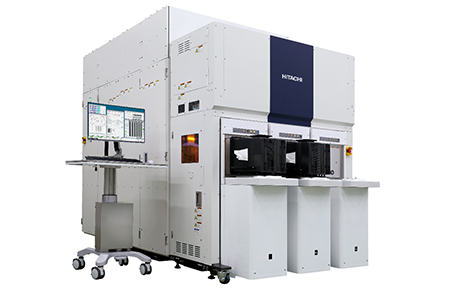
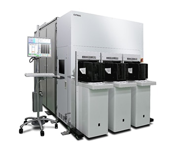
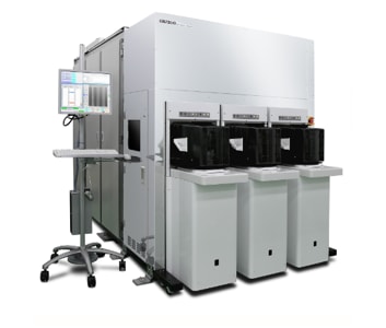
High-Precision Electron Beam Metrology System GT2000
CD-SEM to meet the needs of semiconductor devices development and mass production in High-NA EUV generation
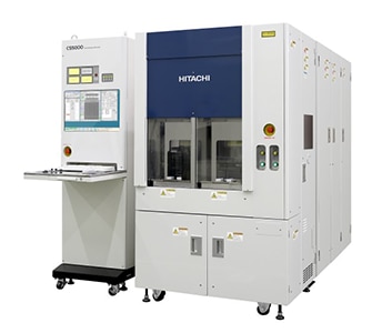
Advanced CD Measurement SEM CS5000
A sustainable CD measurement solution to a wide range of 4, 6, and 8 inch wafer Fabs