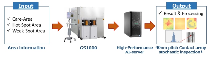
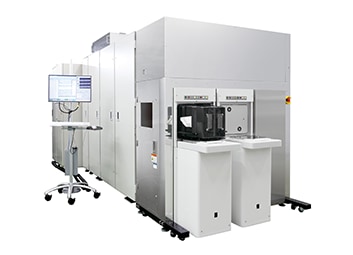
Advanced Area Inspection SEM GS1000
Features
- A new concept inspection and metrology system that combined high-speed wide-area scanning technology with large-current electron beam, and added high-performance processing server.
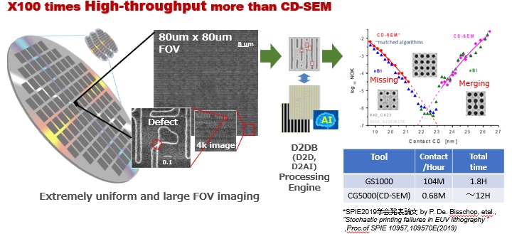
- Achieved high-quality-imaging that a high-resolution 80um x 80um wide-range batch image and <0.02% in-image uniformity accuracy by aberration correction and scan distortion correction technology.
- Multiple process correlation and yield analysis applications are realized by various high-speed massive inspection and metrology using the comparison method between SEM image and design data.
- A high-speed, advanced process yield management system is planned to develop that integrates artificial intelligence (AI) technology.