Electron Beam Absorbed Current (EBAC) Characterization System nanoEBAC NE4000
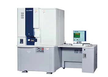
The Hitachi NE4000 nanoEBAC is an electron beam based probing system for electrical characterization and EBAC analysis and imaging of microelectronic device interconnects, materials, and components.
Overview
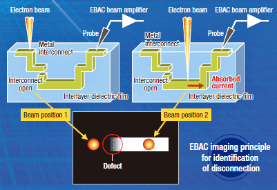
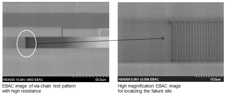
Electron Beam Absorbed Current (EBAC) technique offers a quick and effective method to identify open circuits, high resistance and shorts along interconnects without direct probing techniques of lower level layers.
The EBAC technique is performed with the electron beam by passing through the dielectric layers down to the lower level metallization layer in order to absorb the electron beam current. The electron beam accelerating voltage of the FESEM controls the probing depth or penetration level through the dielectric layers. A single probe is placed on the exposed, upper layer metallization to complete the circuit and allow the electrons to flow through the interconnect.
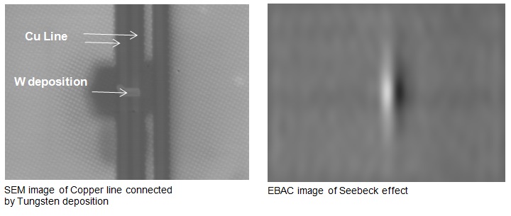
Observation of high resistance and shorts due to Seebeck effect is possible by using dual probes along with the Hitachi patented differential EBAC amplifiers.
User-Friendly Design
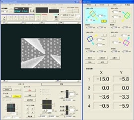
- Intuitive GUI(Graphical User Interface) with various image and color processing functions.
- Coarse positioning of probes are accomplished by an integrated in-chamber CCD camera system.
Premium Image Quality
- Provides high quality EBAC images with Hitachi's patented high performance EBAC amplifiers.
Outstanding Performance
- Field Proven, low chromatic aberration, Cold Field Emission (CFE) electron gun for low accelerating voltage imaging and beam damage reduction of the circuit.
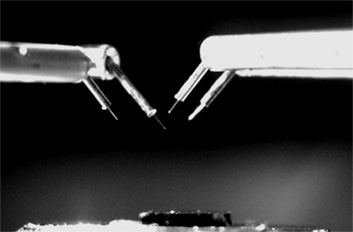
- High precision nano-probe units.
Advanced Applications
- Dedicated nano-probing system with EBAC analysis and electrical characteristics analysis. Large specimen stage can provide fine material and electronics components evaluation.
Specifications
Hitachi Electron Beam Absorbed Current(EBAC) Characterization System nanoEBAC NE4000
| Probe unit | |
|---|---|
| Unit number | 4 |
| Driving method | Piezoelectric |
| Fine stroke range | 5 µm (X,Y) |
| Coarse stroke range | 6 mm (X,Y) |
| Specimen stage / Base stage | |
| Specimen size | 25 mm × 25 mm × 1 mm thick or less |
| Traverse position | Measurement / Specimen exchange position |
| Specimen exchange | Air-locked exchange chamber |
| Prober navigation | Stage traverse to probe position |
| Measurement position memory | |
| Probe coarse adjustment | |
| CCD image display | Image display from lateral direction |
| Electron optics | |
| Electron gun | Cold field emission electron source |
| Accelerating voltage | 0.5 kV to 30 kV |
| Resolution | 15 nm (at 2 kV, WD=15 mm) |
| Image shift | ±150 µm (at 2 kV, WD=15 mm) |
| EBAC amplifier / Image display | |
| Amplifier type | Current amplifier / Differential amplifier |
| Image display | SEM / EBAC (Single / Parallel / Overlay) |
| Image processing | Black and white reversal display, color display, brightness adjustment, slow scan integration, belt scan |
Dimensions and Weight
| Main unit | 1,100 (W) × 1,550 (D) × 1,750 (H) mm, 850 kg |
|---|---|
| Display unit | 1,000 (W) × 1,005 (D) × 1,200 (H) mm, 265 kg |
Utility requirement
| Room temperature | 15 - 25 °C |
|---|---|
| Humidity | 60% RH or less |
| Power | AC100 V±10% 5 kVA (M5 crimp terminal) |
| Grounding | 100Ω or less |
Features
User-Friendly Design
Premium Image Quality
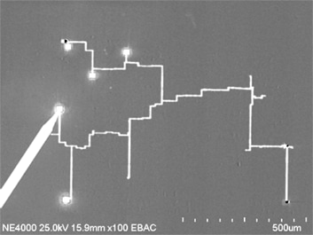
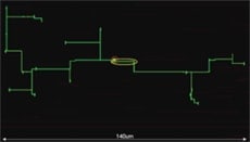
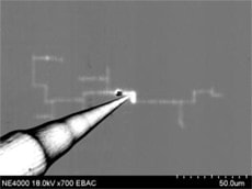
EBAC image of LSI’s net using Hitachi’s original EBAC amplifier
(courtesy of Renesas electronics corporation)
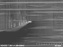
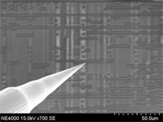
Outstanding Performance
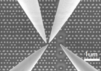
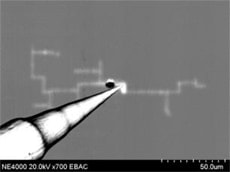
High quality and high resolution imaging with refined nano-probe precision
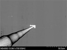
Application Data
EBAC analysis of Via-Chain test pattern with high resistance
EBAC image of Seebeck effect from two dissimilar metals with junctions
EBAC image visualization of multiple layers at various electron accelerating energies