
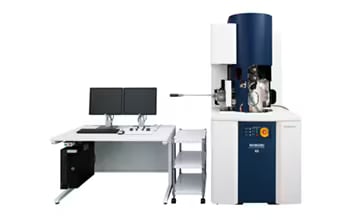
Real-time 3D analytical FIB-SEM NX9000
FIB-SEM System for True 3D Structural Analysis
The newly developed FIB-SEM system from Hitachi, the NX9000 incorporates an optimized layout for true high-resolution serial sectioning to tackle the latest demands in 3D structural analysis and for TEM and 3DAP analyses. The NX9000 FIB-SEM system allows the highest precision in material processing for a wide range of areas relating to advanced materials, electronic devices, biological tissues, and a multitude of other applications.
Features
- The SEM column and FIB column are orthogonally arranged to optimize the column positioning for 3D structural analysis.
- The combination of high-brightness cold-field-emission electron source and high-sensitivity optics support analysis of a wide range of materials from biological tissues to magnetic materials.
- The Micro-sampling system and Triple Beam system allow high-quality sample preparation for TEM and atom-probe applications.
Ion milling and observation at normal incidence in real-time for true analytical imaging
The SEM column and FIB column are orthogonally arranged to realize normal incident SEM imaging of FIB cross sections.
Orthogonal column arrangement eliminates aspect deformation, foreshortening of cross-sectional images, and shift of the field of view (FOV) during serial section imaging, which cannot be avoided by conventional FIB-SEM systems. The NX9000 images enable highly accurate 3D structural analysis. Optical correlative microscopy can be applied easily due to the benefit of surface-planar EM imaging.
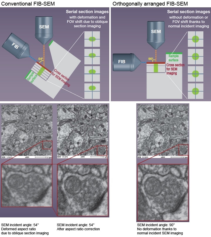
Sample: Mouse brain neuron
Sample courtesy of Yoshiyuki Kubota, Ph.D., Neural Information Processing Systems (NIPS)
Cut & See·3D-EDS*1·3D-EBSD*1 available for a wide variety of materials
Cut&See
Cut & See supports high-resolution, high-contrast imaging of biological tissues, semiconductors, and magnetic materials, such as steel and nickel, at low accelerating voltages.
Serial section images can be collected with high throughput due to the proper geometry of the ion and electron column.
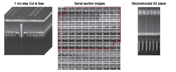
Sample: NAND flash memory
SEM accelerating voltage: 1 kV
Cutting interval: 1 nm
Number of cut: 300
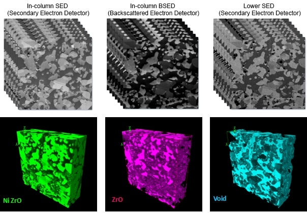
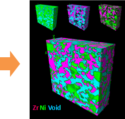
3D-EDS*1
Serial section SEM images and serial section elemental maps can be collected using 3D-EDS.
The large-area silicon drift detector reduces the acquisition time and enables elemental mapping at low accelerating voltages.
Sample: Fuel cell electrode
SEM accelerating voltage: 5 kV
Cutting interval: 100 nm
Number of cut: 212
Sample courtesy of Prof. Naoki Shikazono, University of Tokyo
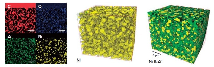
3D-EBSD*1
Simultaneous SEM, FIB, and EBSD signals are obtained for 3D-EBSD without moving the stage during FIB sectioning and EBSD analysis. Accuracy and throughput of 3D crystal orientation analysis and segmentation yield high quality and less post-processing correction.
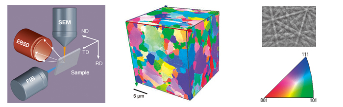
Sample: Ni
SEM accelerating voltage: 20 kV
Cutting interval: 150 nm
Number of cut: 150
*1: Option
Specifications
| Items | Description | |
|---|---|---|
| SEM | Electron source | Cold cathode field emission source |
| Accelerating voltage | 0.1 - 30 kV | |
| Resolution | 2.1 nm@1 kV | |
| 1.6 nm@15 kV | ||
| FIB | Ion source | Ga liquid metal ion source |
| Accelerating voltage | 0.5 - 30 kV | |
| Resolution | 4.0 nm@30 kV | |
| Maximum probe current | 100 nA | |
| Standard detector | In-column SED/In-column BSED/Chamber SED | |
| Stage | X | 0 - 20 mm *2 |
| Y | 0 - 20 mm *2 | |
| Z | 0 - 20 mm *2 | |
| θ | 0 - 360° *2 | |
| τ | -25 - 45° *2 | |
| Maximum sample size | 6 mm x 6 mm, 2 mm thick | |
*2: Stroke is limited by each sample holder
The NANOMESH grid for FIB processing alleviates redeposit effects for high quality lamella preparation.
Numerous locations for mounting lamellae allows for high precision sample preparation and material features for better analysis.
Application Data
Material Science
3D distribution analysis with multiple signals
Specimen: Fuel cell electrode SEM accelerating voltage: 0.3 kV
FOV: 20 µm
Cutting interval: 10 nm
Number of cut: 600
Semiconductor
3D structural analysis from serial section SEM images
Specimen: 3D NAND flash memory
High-precision site-specific lamella preparation
30 kV FIB
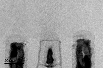
1 kV Ar
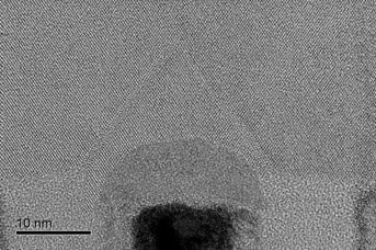
Specimen: 14 nm SoC device
Final milling: 1 kV Ar
Observation: HF-3300 Cold FE-TEM (Accelerating voltage: 300 kV)
Life science
3D reconstruction from serial section SEM images
Specimen: Mouse brain neuron