
Lead (Pb) in Thin Film Samples
We know that electroless nickel phosphorus plating and Pb-free solder plating contain small amounts of Pb that must be controlled as a hazardous element. Hitachi High-Tech Analysis developed the Thin Film FP method for accurate measurement of plating samples.
Measurement of Electro-less Ni Plating
The table and figure below shows excellent results of 10 readings of approximately 350ppm of Pb in Ni-P plating (5um) over cupper. The correlation of Pb is less than 3%. The readings correlate well with ICP values.
Measurement Conditions (SEA1200VX)
Method: Thin Film FP
Beam Size: φ8.0mm
Voltage: 50kV
Current: Auto
Atmosphere: Air
Primary Filter: For Pb
Sample
Electro-less Ni Plating 5µm
ICP Result
Pb 363ppm
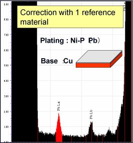
10 Reading from SEA1200VX
| Ni-P(µm) | Pb(ppm) | |
|---|---|---|
| Ave. | 5.54 | 334 |
| STDEV | 0.26 | 8.66 |
| CV% | 4.68 | 2.59 |
Measurement of Pb Free Solder
Pb-free solder plating also contains a small amount of Pb. The table and figure below show excellent results from one reading of a Pb measurement in Pb-free solder plating 5 micro meters in thickness. The CV value of Pb concentration was less than 3% and the reading also correlates well with ICP.
Measurement Conditions (SEA1200VX)
Method: Thin Film FP
Beam Size: φ8.0mm
Voltage: 40kV, 50kV
Current: Auto
Atmosphere: Air
The Primary Filter: For Pb & For Cd
Sample
Pb in Pb Free Solder 5µm
ICP Result
Pb 312ppm
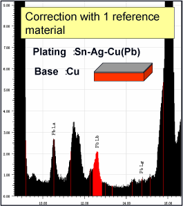
10 Reading from SEA1200VX
| Sn-Ag(µm) | Pb(ppm) | |
|---|---|---|
| Ave. | 5.5 | 348 |
| STDEV | 0.02 | 8.95 |
| CV% | 0.27 | 2.57 |