초고분해능 전계방출형 주사전자현미경 SU9000
Cold FE 전자원은 여타 전자원 대비 광원 크기나 에너지 폭이 작아서 고분해능 관찰에 적합합니다. 아울러 SU9000은 고휘도와 안전성을 겸비한 신형 Cold FE 전자총을 탑재하여 고분해능 관찰만 아니라 고품질 원소 분석 또한 가능합니다.
또한, In-lens형 대물 렌즈를 갖춘 SU9000은 Option장착으로 EELS 및 Diffraction 측정이 가능해졌습니다.
특징
SU9000은 히타치 FE-SEM의 최상위 기종입니다.
저수차 렌즈의 최고봉인 In-lens형 대물 렌즈를 탑재한 SU9000은 세계 최고 분해능 0.4 nm (가속 전압 30 kV) 를 달성하였습니다. 저가속전압 영역에서는 0.8 nm (조사 전압 1 kV) 를 보증하고 있습니다.
SU9000은 High-end TEM과 동일한 Side Entry Stage를 채용하고 있습니다. 아울러 고강성 Frame과 소음 차단 커버를 통해 다양한 설치 환경에서도 높은 퍼포먼스를 실현합니다.
또한, SU9000의 시료실은 종래 대비 한 차원 높은 진공을 유지할 수 있으므로 Contamination의 영향을 최소한으로 억제할 수 있습니다.
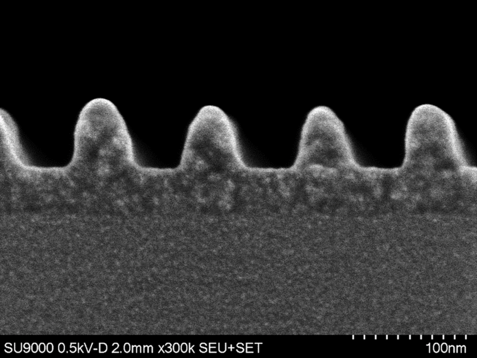
Vacc : 500 V
Signal : SE image
With beam deceleration
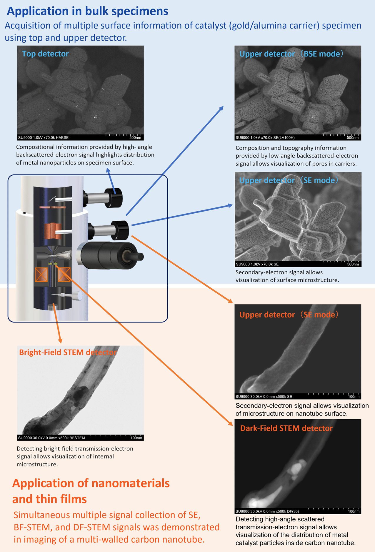
SU9000의 Imaging용 검출기는 Upper / Top / BF-STEM / DF-STEM 4종을 장착할 수 있습니다.
히타치 FE-SEM에서 정평이 난 Super ExB 필터는 Upper 검출기와의 조합을 통하여 SE 및 LA-BSE를 제어합니다. 이를 통해 표면의 미세 구조 관찰이나 조성 관찰이 가능합니다.
Top 검출기에서는 HA-BSE를 검출함으로써 요철 정보를 저감한 반사전자 Image (조성, 결정)을 취득할 수 있습니다. 이러한 검출기들을 갖추고 있는 SU9000은 촉매 등 최첨단 연구에 적합한 시스템입니다.
아울러 SU9000의 STEM 기능은 박막 시료와 밀도차의 작은 시료 등 High-Contrast 관찰에 최적입니다. 또한, BF / DF Duo-STEM 검출기 (옵션)는 명시야 Image와 암시야 Image를 동시에 취득할 수 있습니다.
안정성이 뛰어난 SU9000은 Graphite의 격자 간격에 해당하는 0.34 nm의 STEM 분해능을 보증하고 있습니다.
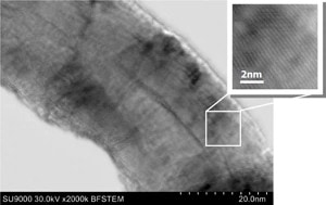
Vacc : 30 kV
Mag. : 2,000 kx
Bright Field (BF)-STEM image
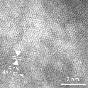
Vacc : 30 kV
Mag. : 3,000 kx
Bright Field (BF)-STEM image
주요 특징
- 0.4 nm@3.0 kV의 세계 최고 2차전자분해능을 보증
- 새롭게 개발한 Cold FE 전자총으로 저수차와 고휘도 안정 Probe 모두를 실현
- 시료 Damage의 경감 등을 목적으로 한 저가속 전압 성능
- Contamination의 영향을 경감한 초고진공시료실
- 다양한 설치 환경 하에서도 높은 퍼포먼스를 실현하기 위한 고강성 Frame과 소음 차단 커버
- Side-entry 방식 (시료 교환 위치가 고분해능 관찰 위치)을 통한 신속한 고분해능 관찰
사양
| 항목 | 내용 | |
|---|---|---|
| 분해능 | ||
| 2차전자분해능*1 | 0.4 nm (가속 전압 30 kV) 0.8 nm (조사전압 1 kV) |
|
| STEM분해능*2 | 0.34 nm | |
| 배율 표시 | ||
| 표시 방법의 전환 기능 | 사진 배율*3 | 실제 표시 배율*4 |
| 저배율 모드 | 80~10,000배 | 220~25,000배 |
| 고배율 모드 | 800~3,000,000배 | 2,200~8,000,000배 |
| 광학계 | ||
| 전자총 | 냉음극전계방출형 전자총 | |
| 가속 전압 | 0.5~30 kV (0.1 kV Step) | |
| 렌즈계 | 3단 전자 렌즈 축소계 | |
| 대물렌즈 조리개 | 가동 조리개 (가열 Type, 진공 밖에서 4공 전환 및 미세 조정 가능) | |
| 전기적 시야 이동 | ±5 µm (Sample Height=0.0 mm) | |
| Beam Blanking | 주사신호동기식 High-speed Blanking System 탑재 | |
| Stage / 시료 사이즈 | ||
| Stage | Side-entry Goniometer Stage | |
| 가동 범위 | X: ±4.0 mm, Y: ±2.0 mm, Z: ±0.3 mm, T: ±40° | |
| 표준 홀더 (1개 부속) | 평면 시료대: 5.0 mm × 9.5 mm × 3.5 mm (높이) (최대) | |
| 시료대 (6종류 × 1개 부속) | 단면 시료대: 2.0 mm × 6.5 mm × 5.0 mm (높이) (최대) | |
| 전용 홀더*2 | 단면 홀더: 2.0 mm × 12.0 mm × 6.0 mm (높이) 대형 단면 2축 경사 홀더: 0.8 mm × 8.5 mm × 5.5 mm (높이) |
|
| 검출기 | ||
| 검출기 | 2차전자검출기 (SE / BSE 신호 검출 비율 변경 기능 탑재) Top 검출기*2 BF / DF Duo-STEM 검출기*2 에너지 분산형 X선 검출기*2 |
|
| 화상 표시 | ||
| 모니터 크기 | 24.1형 와이드 LCD (표시 화소: 1,920 × 1,200) | |
| 대화면 표시 | 1,280 × 960화소 | |
| 1화면 / 2화면 표시 | 800 × 600화소 / 800 × 600화소×2 | |
| 4화면 표시 | 640 × 480화소×4 | |
| 제어계 | ||
| OS | Windows®10 | |
| 조작 방법 | PC 모니터 상의 GUI, 표시 전환 (일본어 / 영어 메뉴) | |
| 조작 Table | 마우스, 키보드, 전용 Rotary Knob, Stage Controller (Trackball / Joystick 복합) | |
| Image 저장 사이즈 | 640 × 480, 1,280 × 960, 2,560 × 1,920, 5,120 × 3,840화소 | |
| Image 저장 데이터 관리 | SEM Manager (Image Data 관리, Thumbnail 표시, 각종 Image 관리 기능) | |
*1 자사 시료의 SEM Image로부터 가장 작은 입자 간 Gap 을 측정
*2 옵션
*3 127 mm × 95 mm (사진 크기 4 × 5) 를 표시 사이즈로 배율을 규정
*4 345 mm × 259 mm (1,280 × 960 화소 표시: 가속 전압 5 kV 이상)를 표시 사이즈로 배율을 규정
LV-STEM
High-Resolution, Analytical STEM/SEM Providing Simultaneous Chemical and Bonding Analysis, Atomic Resolution, and Surface Imaging at 30kV and below
Investigating samples with the full capabilities of STEM at 30 keV and below is an extremely interesting and rapidly growing area of research: providing both Materials and Life Sciences with full SEM and STEM, inclusive EDX, and EELS capabilities, at low voltages. Less beam damage and higher contrast are the key arguments for the Low-Voltage STEM (LV-STEM), a capability that has been out of reach for researchers globally. With the LV-STEM, its low beam energy, increased contrast, and narrow energy spread, investigations of biological material in an unstained condition are becoming a reality for the first time.
Since the STEM unit has no imaging lens after the sample, electrons that were inelastically scattered by the sample do not really worsen image quality (they do for TEM). The significance of the lack of chromatic aberrations after the sample increases with decreasing electron energy; samples that typically would require a 100-keV TEM, at the very least, can be investigated with low-keV STEM. Multi-scattering processes and absorption of course still appear—ultimately limiting the acceptable thickness of the specimen. However, the use of high-end specimen preparation techniques, or working with thin samples as is typical in nano-research fields, allows 30-keV STEMs to cover much of the areas of conventional higher-keV TEMs, while at the same time, providing surface information through standard SEM methods, including SE, BSE, and high-angle BSE.
The well-established cold FEG of Hitachi’s high-end SEMs is a tremendous benefit for EELS capabilities as well as the point resolution of STEM. Despite the unusually low voltage for EELS and the increased impact of environmental conditions on low-voltage electrons, we are able to demonstrate better than 400-meV FWHM (full width half maximum, see Figure 1, left) for the ZLP (zero loss peak) of EELS, allowing clear and crisp EELS data for fine structure investigations. For example, eliciting the tiny changes in the π bonding for the Graphene as layer after layer is added demonstrates the sensitivity of the LV-STEM (see Figure 1, right). The LV-STEM also has a 2nd dedicated EELS detector with 3 elements, allowing the rapid (10,000 fps) acquisition of energy-filtered BF STEM images, Plasmon images, or the rapid collection of elemental maps. Switching between both detectors is easy and relies on Hitachi’s own unique design.
The LV-STEM feature (Figure 2) complements SE imaging and makes no compromise. Typical images taken at 30 keV without a Cs corrector or Cc corrector approach 0.2-nm resolution establishing the LV-STEM as the true performance leader for ≤ 30 keV microscopy. The importance of simultaneously acquiring STEM and SE data is demonstrated in Figure 3.
As this microscope can handle samples up to 5.0 mm × 9.5 mm × 3.5 mm, the optional windowless EDX detector supports the analysis of both thin and bulk areas. At an incredible collection angle of 0.7 sr, acquisition times for EDX maps are short (see details in Figure 4), making the LV-STEM a truly ground-breaking microscope for both Materials and Life Sciences applications.
References
- R.F. Egerton, “Electron Energy-Loss Spectroscopy in Electron Microscope”, Springer, New York
- K. Suenaga et al., Nature, Vol.468 (2010), 1088-1090
- G. Algara-Siller, O. Lehtinen, A. Turchanin and U. Kaiser, (2014). Appl. Phys. Lett., 104, 153115.
- The authors wish to thank Dr. Tsuyohiko Fujigaya, Kyushu University for providing the samples.
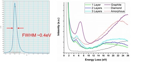
Figure 1 Left: despite the low (± 30 keV) energy of these electrons, the energy spread of the electron beam, measured by our own Hitachi EELS is 400 meV or less:. Right: EELS spectra differentiating between single , double and triple layers of graphene , graphite, diamond, and amorphous carbon.
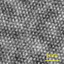
Figure 2 The low-pass-filtered BF STEM of Graphene at 30 keV shows a resolution of close to 0.2 nm; the 0.142 nm atom distances are not resolved.
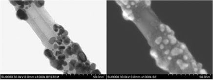
Figure 3 Left: The high-resolution 30-keV BF STEM image by itself makes it difficult to model its 3D structure. Right: Only in combination with the (simultaneously acquired) high-resolution SE image, the real structure of this sample becomes obvious and modeling this structure as a 3D model would be quite manageable.
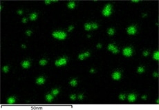
Figure 4 Elemental EDX map (Au M) at 30 kV, The size of the nano-particles is in the range of 5-10 nm. Acquisition time is 3.5 min at a current of 1 nA
PDF 형식의 파일을 확인하시려면, Adobe Systems InIncorporated(Adobe Systems社)의Adobe® Reader®가 필요합니다.
Information on our new cold field emitter technology can be found here.
Hitachi FE-SEM Application Data
This journal addresses a wide range variety of research papers and useful application data using Hitachi science instruments.
Photo collections of beauty of metals, minerals, organisms etc. reproduced by the electron microscope and finished more beautifully by computer graphic technology.
Related Product Categories
Related Links
관련 정보