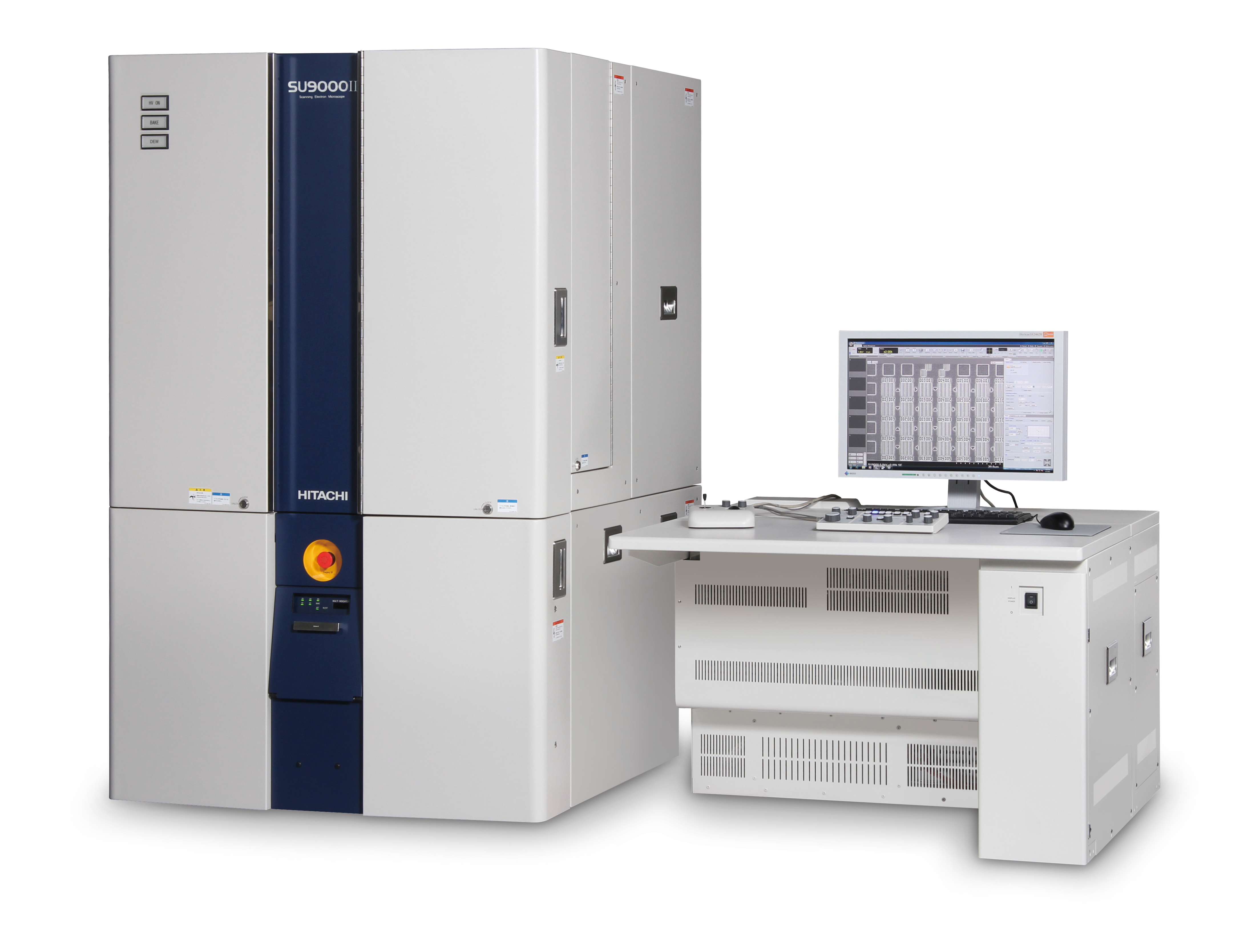
超高分解能電界放出形走査電子顕微鏡 SU9000II
コールドFE電子源は、他の電子源と比べて光源径やエネルギー幅が小さいので、高分解能観察に適しています。さらに高輝度かつ安定性な新型コールドFE電子銃を搭載したSU9000IIは高分解能観察のみならず、高品質な元素分析が可能です。それらの性能を発揮したデータを安定して取得できるよう、光学系の自動調整機能やデータ取得自動化を支援するオプション機能を搭載し、大量データの自動取得を可能にしました。
また、インレンズ形対物レンズを備えたSU9000IIは、EELSの測定が可能です。
SU9000を用いた低加速EELSとDiffractionについては、この記事を参照ください。
* doi:10.1017/S1431927616003871, Microsc. Microanal. 22 (Suppl 3), 2016, © Microscopy Society of America 2016
価格:お問い合わせください
取扱会社:株式会社 日立ハイテク
特長
日立FE-SEMの最上位機種
SU9000IIは日立FE-SEMの最上位機種です。
低収差レンズの最高峰であるインレンズ型対物レンズを搭載したSU9000IIは、世界最高分解能 0.4 nm(加速電圧 30 kV)を達成しました。低加速電圧領域では0.7 nm(照射電圧:1.0 kV/オプション)を保証しています。
SU9000IIはハイエンドTEMと同様のサイドエントリーステージを採用しています。さらには高剛性フレームと耐騒音カバーによってさまざまな設置環境においても高いパフォーマンスを実現します。
加えて、SU9000IIの試料室は、従来と比べて一桁高い真空を保持できるのでコンタミネーションの影響を最小限に抑えることができます。
それらの性能を発揮したデータを安定して取得できるよう、SU9000Ⅱでは光学系の調整自動化機能を搭載し、連続データ取得をはじめとした、データ取得の自動化を支援するオプションソフト「EM Flow Creator」が搭載可能です。
Vacc : 500 V
Signal : SE image
With beam deceleration
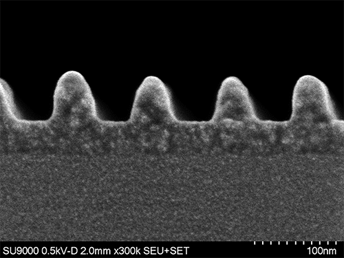
SU9000IIのインレンズ型対物レンズは短焦点距離化による収差低減に有効な構造を有しています。
収差低減によって分解能が向上したことで、数nm以下の微細構造もより安定して観察が可能になりました。
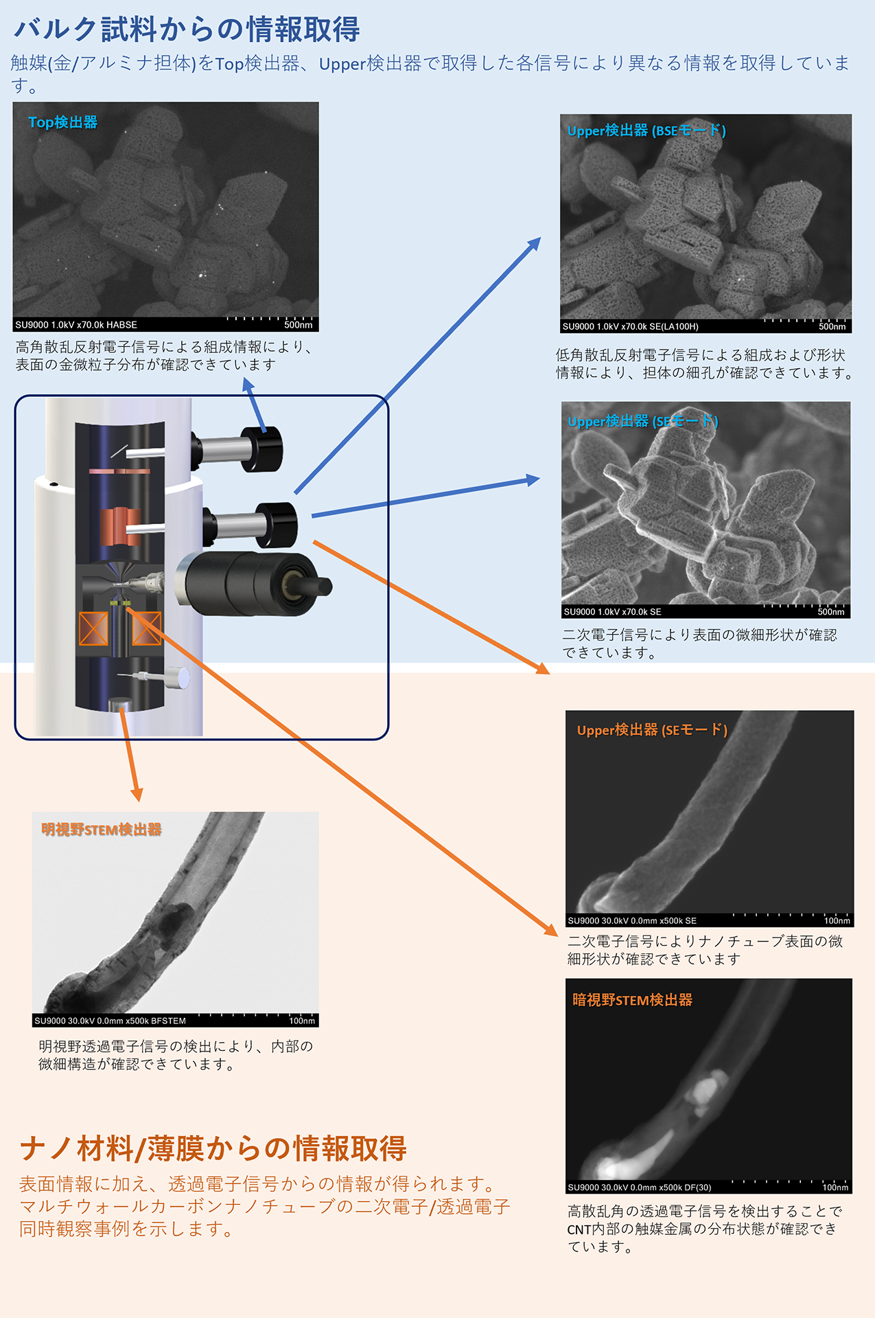
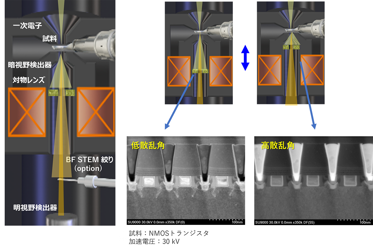
低加速STEMの新たな可能性を拓く
散乱角を選択した暗視野STEM像
BF/DF Duo-STEM検出器(オプション)
SU9000IIに装着可能なBF/DF Duo-STEM検出器の暗視野では散乱角を選択した信号取得が可能です。試料と暗視野検出器面の距離を制御することでHAADF条件での観察が可能になり、Z-コントラストを強調した信号を取得できます。
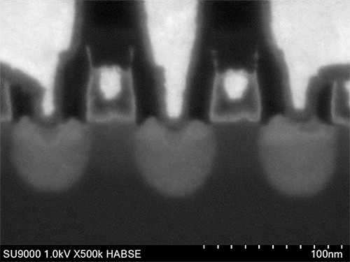
SEM/STEMによる格子像観察
SU9000IIの持つ、低収差のインレンズ型対物レンズおよびSTEM観察に適した光学系の構造はSEM/STEMの観察手法を拡張しました。
照射電子線の収束角を制御し、透過電子の検出面に干渉縞を発生させることによってSEM/STEMでの格子像が観察可能です。
右図は葉ろう石(pyrophyllite)の明視野STEM像です。(020)の0.445 nmの格子縞が観察できています。
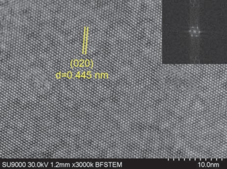
加速電圧:30 kV
主な特長
- 30 kVで0.4 nmの世界最高の二次電子分解能を保証
- 低収差と高輝度安定プローブ電流を両立した新開発コールドFE電子銃
- 試料ダメージの軽減などを目的とした低加速電圧性能
- 新たに0.7 nm(照射電圧:1.0 kV/オプション)を保証
- 光学系の自動調整機能やデータ取得自動化を支援するオプション機能を搭載し、大量データの自動取得を可能にしました。
- コンタミネーションの影響を軽減させた超高真空試料室
- さまざまな設置環境下でも、高いパフォーマンスを実現するための高剛性フレームと耐騒音カバー
- サイドエントリー方式(試料交換位置が高分解能観察位置)による迅速かつ高分解能観察
仕様
| 項目 | 内容 | |
|---|---|---|
| 分解能 | ||
| 二次電子分解能 | 0.4 nm(加速電圧 30 kV) 0.7 nm (照射電圧1kV)*1 |
|
| STEM分解能*2 | 0.34 nm | |
| 倍率表示 | ||
| 表示方法の切替機能 | 写真倍率*3 | 実表示倍率*4 |
| 低倍率モード | 80~10,000倍 | 220~25,000倍 |
| 高倍率モード | 800~3,000,000倍 | 2,200~8,000,000倍 |
| 光学系 | ||
| 電子銃 | 冷陰極電界放出形電子銃 | |
| 加速電圧 | 0.5~30 kV(0.1 kVステップ) | |
| レンズ系 | 3段電磁レンズ縮小系 | |
| 対物レンズ絞り | 可動絞り(加熱タイプ、真空外より4孔切替及び微調整可能) | |
| 電気的視野移動 | ±5 µm(Sample Height=0.0 mm) | |
| ビームブランキング | 走査信号同期式ハイスピードブランキングシステム搭載 | |
| 電子光学系自動調整機能 | オートブライトネス&コントラスト(ABCC) オートフォーカス(AFC) オートスティグマ(ASC) オートビームアライメント (ABA) オートアパーチャアライメント (AAA) オートスティグマアライメント (ASA) |
|
| ステージ/試料サイズ | ||
| ステージ | サイドエントリーゴニオメーターステージ | |
| 可動範囲 | X:±4.0 mm、Y:±2.0 mm、Z:±0.3 mm、T:±40° | |
| 標準ホルダー(1本付属) | 平面試料台:5.0 mm×9.5 mm×3.5 mm(高さ) (最大) | |
| 試料台(6種類×1個付属) | 断面試料台:2.0 mm×6.5 mm×5.0 mm(高さ) (最大) | |
| 専用ホルダー*2 | 断面ホルダー:2.0 mm×12.0 mm×6.0 mm(高さ) 大型断面2軸傾斜ホルダー:0.8 mm×8.5 mm×5.5 mm(高さ) |
|
| 検出器 | ||
| 検出器 | 二次電子検出器(SE/BSE信号 検出比率可変機能付) Top検出器*2 BF/DF Duo-STEM検出器*2 エネルギー分散型X線検出器*2 |
|
| 画像表示 | ||
| モニタサイズ | 24.1型ワイドLCD(表示画素:1,920×1,200) | |
| 大画面表示 | 1,280×960画素 | |
| 1画面/2画面表示 | 800×600画素/800×600画素×2 | |
| 4画面表示 | 640×480画素×4 | |
| 制御系 | ||
| 操作方法 | PCモニタ上のGUI、表示切替(日本語/英語メニュー) | |
| 操作卓 | マウス、キーボード、専用ロータリーノブ、ステージコントローラ(トラックボール/ジョイスティック複合) | |
| 保存画像サイズ | 640×480、1,280×960、2,560×1,920、5,120×3,840画素 | |
| 保存画像データ管理 | SEMマネージャ(画像データ管理、サムネイル表示、各種画像処理機能) | |
*1
リタ―ディング機能ユニット(オプション)使用時。
1 kV分解能数値はリタ―ディング用平面ホルダー/Top検出器(オプション)使用時の値です
*2 オプション(電源ケーブル先端は3Pコンセント、M5圧着端子、M6圧着端子のいずれかを選択)
*3 127 mm×95 mm(4×5写真サイズ)を表示サイズとして倍率を規定
*4 345 mm×259 mm(1,280×960画素表示:加速電圧5 kV以上)を表示サイズとして倍率を規定
LV-STEM
High-Resolution, Analytical STEM/SEM Providing Simultaneous Chemical and Bonding Analysis, Atomic Resolution, and Surface Imaging at 30kV and below
Investigating samples with the full capabilities of STEM at 30 keV and below is an extremely interesting and rapidly growing area of research: providing both Materials and Life Sciences with full SEM and STEM, inclusive EDX, and EELS capabilities, at low voltages. Less beam damage and higher contrast are the key arguments for the Low-Voltage STEM (LV-STEM), a capability that has been out of reach for researchers globally. With the LV-STEM, its low beam energy, increased contrast, and narrow energy spread, investigations of biological material in an unstained condition are becoming a reality for the first time.
Since the STEM unit has no imaging lens after the sample, electrons that were inelastically scattered by the sample do not really worsen image quality (they do for TEM). The significance of the lack of chromatic aberrations after the sample increases with decreasing electron energy; samples that typically would require a 100-keV TEM, at the very least, can be investigated with low-keV STEM. Multi-scattering processes and absorption of course still appear—ultimately limiting the acceptable thickness of the specimen. However, the use of high-end specimen preparation techniques, or working with thin samples as is typical in nano-research fields, allows 30-keV STEMs to cover much of the areas of conventional higher-keV TEMs, while at the same time, providing surface information through standard SEM methods, including SE, BSE, and high-angle BSE.
The well-established cold FEG of Hitachi’s high-end SEMs is a tremendous benefit for EELS capabilities as well as the point resolution of STEM. Despite the unusually low voltage for EELS and the increased impact of environmental conditions on low-voltage electrons, we are able to demonstrate better than 400-meV FWHM (full width half maximum, see Figure 1, left) for the ZLP (zero loss peak) of EELS, allowing clear and crisp EELS data for fine structure investigations. For example, eliciting the tiny changes in the π bonding for the Graphene as layer after layer is added demonstrates the sensitivity of the LV-STEM (see Figure 1, right). The LV-STEM also has a 2nd dedicated EELS detector with 3 elements, allowing the rapid (10,000 fps) acquisition of energy-filtered BF STEM images, Plasmon images, or the rapid collection of elemental maps. Switching between both detectors is easy and relies on Hitachi’s own unique design.
The LV-STEM feature (Figure 2) complements SE imaging and makes no compromise. Typical images taken at 30 keV without a Cs corrector or Cc corrector approach 0.2-nm resolution establishing the LV-STEM as the true performance leader for ≤ 30 keV microscopy. The importance of simultaneously acquiring STEM and SE data is demonstrated in Figure 3.
As this microscope can handle samples up to 5.0 mm × 9.5 mm × 3.5 mm, the optional windowless EDX detector supports the analysis of both thin and bulk areas. At an incredible collection angle of 0.7 sr, acquisition times for EDX maps are short (see details in Figure 4), making the LV-STEM a truly ground-breaking microscope for both Materials and Life Sciences applications.
References
- R.F. Egerton, “Electron Energy-Loss Spectroscopy in Electron Microscope”, Springer, New York
- K. Suenaga et al., Nature, Vol.468 (2010), 1088-1090
- G. Algara-Siller, O. Lehtinen, A. Turchanin and U. Kaiser, (2014). Appl. Phys. Lett., 104, 153115.
- The authors wish to thank Dr. Tsuyohiko Fujigaya, Kyushu University for providing the samples.
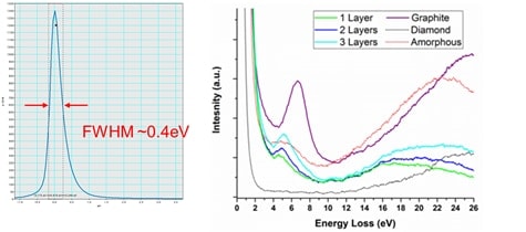
Figure 1 Left: despite the low (± 30 keV) energy of these electrons, the energy spread of the electron beam, measured by our own Hitachi EELS is 400 meV or less:. Right: EELS spectra differentiating between single , double and triple layers of graphene , graphite, diamond, and amorphous carbon.
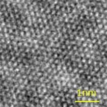
Figure 2 The low-pass-filtered BF STEM of Graphene at 30 keV shows a resolution of close to 0.2 nm; the 0.142 nm atom distances are not resolved.
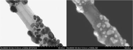
Figure 3 Left: The high-resolution 30-keV BF STEM image by itself makes it difficult to model its 3D structure. Right: Only in combination with the (simultaneously acquired) high-resolution SE image, the real structure of this sample becomes obvious and modeling this structure as a 3D model would be quite manageable.
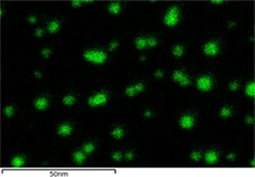
Figure 4 Elemental EDX map (Au M) at 30 kV, The size of the nano-particles is in the range of 5-10 nm. Acquisition time is 3.5 min at a current of 1 nA
PDF形式のファイルをご覧になるには、Adobe Systems Incorporated (アドビシステムズ社)のAdobe® Reader®が必要です。
弊社製品を使用した社内外の研究論文、技術情報、アプリケーションおよび新製品情報を公開しています。
・技術機関誌 SI NEWSの関連記事のご案内
1958年の創刊以来、SI NEWS(エスアイニュース)は、弊社製品を使用した社内外の研究論文、アプリケーションおよび新製品情報を公開しています。
超高分解能電界放出形走査電子顕微鏡 SU9000の記事のご案内です。
「戦後イノベーション100選」は、公益社団法人発明協会が創立110周年を迎えたことを記念し、戦後日本で成長を遂げ、産業経済の発展に大きく寄与したイノベーションを選定したものです。
日立ハイテクの「電界放出形電子顕微鏡」は、7月8日に行われた第一回発表において、戦後復興期から高度経済成長期までの38件のイノベーションの一つとして選定されました。
日立ハイテクは、今回の「戦後日本のイノベーション100選」に選定された電界放出形電子顕微鏡をはじめ、今後も優れた技術・製品の開発を通じて、安心・安全で快適な社会の実現および世界の産業の発展に貢献していきます。
-日立電界放出形走査電子顕微鏡/キュレーション(惑星物質試料受け入れ)設備のご紹介-
46億年前の太陽系の化石ともいわれる小惑星イトカワの微粒子。 地球物質の影響を遮断した環境でのナノ解析がスタートしました。
FE-SEMの測定例を紹介します。
電子顕微鏡・FIBなどに関するセミナーを紹介します。
電子顕微鏡により忠実に再現した、金属、鉱物、生物などの造形の美をコンピュータのグラフィック技術により、さらに美しく仕上げた写真集です。
年表で見る日立の電子顕微鏡の歩みを紹介します。
電子顕微鏡の観察に関するポイントなど田中先生の「秘伝」を伝授いただきました。
関連情報