
Analytical Services with Transmission Electron Microscopy (TEM)
Hitachi High-Tech America has a state-of-the art microscopy lab in Hillsboro, Oregon. Using innovative Transmission Electron Microscopes (TEM), dedicated equipment and a staff of full-time, industry-experienced engineers work on samples for various applications including but not limited to:
- Nanotechnology and quantum devices
- Materials science (metals, ceramics, polymers)
- Semiconductor device failure analysis
- Advanced biological studies
- Thin-film characterization for electronics and optoelectronics
Available Instruments
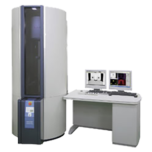
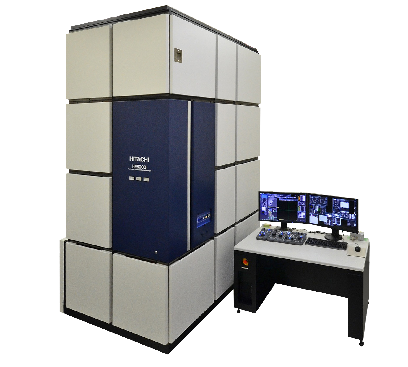
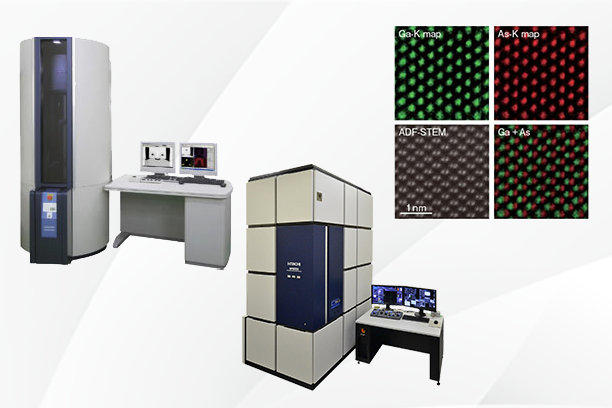
Transmission Electron Microscopes (TEM)
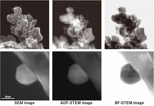
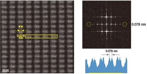
- Atomic-Scale Imaging: TEM provides unprecedented resolution down to the atomic scale, ideal for studying the internal structure of materials.
- Crystallographic Analysis: With diffraction capabilities, TEM allows detailed analysis of crystalline structures, including lattice spacing, orientation, and defects.
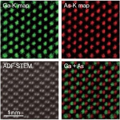
- High-Resolution Elemental Mapping: Through techniques like Electron Energy Loss Spectroscopy (EELS) and Energy-Dispersive X-ray Spectroscopy (EDX), TEM provides chemical mapping at the atomic level.
- Thin-Film Analysis: Characterize thin films, interfaces, and layered materials with precise measurements of thickness and composition.
Applications
- Nanotechnology and quantum devices
- Materials science (metals, ceramics, polymers)
- Semiconductor device failure analysis
- Advanced biological studies
- Thin-film characterization for electronics and optoelectronics