
Analytical Services with Focused Ion Beam (FIB/FIB-SEM)
Hitachi High-Tech America has a state-of-the art microscopy lab in Hillsboro, Oregon. Using innovative Focused Ion Beam (FIB), dedicated equipment and a staff of full-time, industry-experienced engineers work on samples for various applications including but not limited to:
- Semiconductor device inspection
- Failure analysis and quality control
- Nanomaterials and coatings
- Geology and mineralogy
- Biomaterials and life sciences
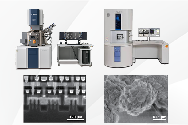
Available Instruments
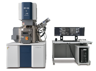
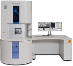
Focused Ion Beam (FIB)
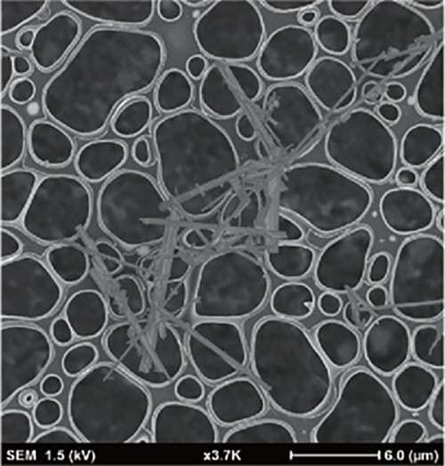
- High-Resolution Imaging: Capture ultra-high-resolution images to visualize surface morphology, texture, and structure at the micron and sub-micron scale.
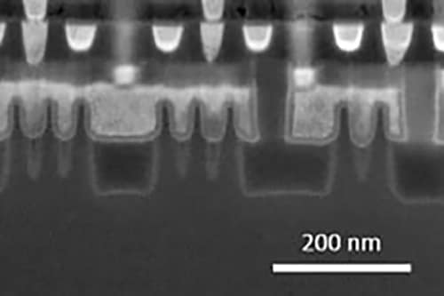
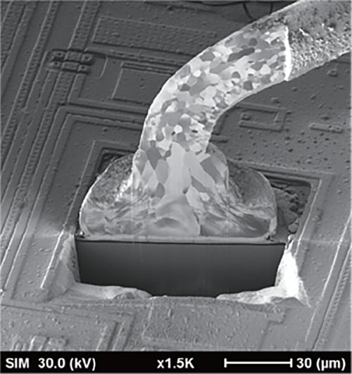
- Accelerated Failure Analysis: FIB-SEM is ideal for investigating microfractures, corrosion, and other defects that can impact the performance and reliability of your materials.
- TEM Sample Preparation: FIB-SEM is the ideal way to prepare samples for TEM analysis. Samples can be thinned to <20nm to endpoint specific features in the nanoscale.
Applications
- Semiconductor device inspection
- Failure analysis and quality control
- Nanomaterials and coatings
- Geology and mineralogy
- Biomaterials and life sciences