
Analytical Services with Critical Dimension Scanning Electron Microscopy (CD-SEM)
Hitachi High-Tech America has a state-of-the art microscopy lab in Hillsboro, Oregon. Using innovative Critical Dimension Scanning Electron Microscopes (CD-SEM), dedicated equipment and a staff of full-time, industry-experienced engineers work on samples for various applications including but not limited to:
- Process Control and Monitoring
- Across-wafer and Local CD Uniformity Characterization
- Line Edge Roughness (LER) and Line Width Roughness (LWR) Analysis
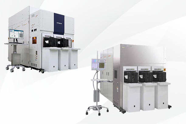
Available Instruments
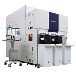
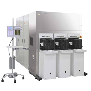
CG6300
Critical Dimension Scanning Electron Microscopy (CD-SEM)
- High Resolution and Precision: CD-SEM provides nanometer-scale resolution, allowing for extremely precise measurement of line widths, spaces, and critical dimensions on semiconductor devices.
- Non-Destructive Measurement: Unlike some metrology tools, CD-SEM allows for non-destructive imaging and measurement, preserving the integrity of the wafer.
- Advanced Image Processing Algorithms: Utilizes sophisticated edge-detection and pattern recognition algorithms to ensure accurate, repeatable, and automated measurements.
- Charge Control and Low-Voltage Imaging: Designed to minimize charging effects on insulating materials (like photoresists) by using low-voltage electron beams and charge neutralization techniques.
Applications
- Process Control and Monitoring
- Across-wafer and Local CD Uniformity Characterization
- Line Edge Roughness (LER) and Line Width Roughness (LWR) Analysis