Electron Microscopes / Atomic Force Microscopes
Select a field

Topics
- News
- Events
Products
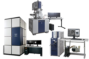
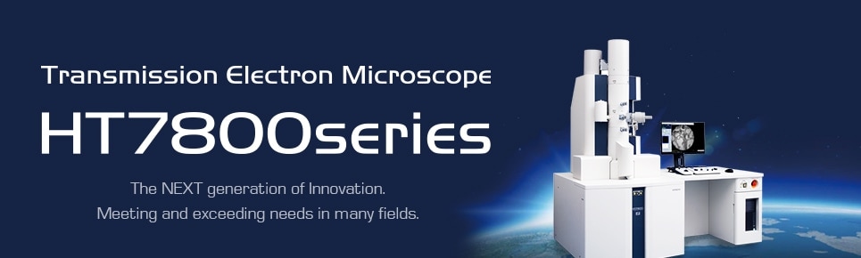
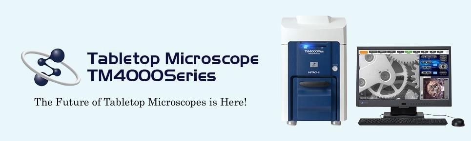
Electron Microscopes
(SEM*1/TEM*2/STEM*3)
Electron Microscopes use electron beam which has shorter wavelength than light to resolve fine structure considered too small for light microscopes. They are used in a wide variety of fields from metals/ceramics/semiconductors to polymers/biological tissues.
TEM and STEM are used to observe internal structure by detecting electrons transmitted through a thin specimen while SEM is used to observe surface structure by detecting electrons generated upon primary electron beam irradiation on the surface of a sample.
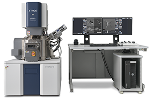
Focused Ion Beam Systems
(FIB*4/FIB-SEM)
FIB is used to observe surface structure by detecting electrons generated upon ion beam irradiation and process the surface of a sample to an arbitrary shape by the use of focused ion beam. Since the ion beam can arbitrarily scan on a sample, FIB is widely used for site-specific cross section preparation for SEM observation and lamella preparation for TEM observation. FIB-SEM incorporates both FIB and SEM in a single system, and allows in-situ SEM observation of FIB-prepared cross section. By repeating FIB milling and SEM observation, serial cross-sectional SEM images can be collected and reconstructed for further three-dimensional structural analysis of the sample.
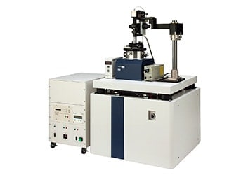
Atomic Force Microscopes (AFM)
Innovative Atomic Force Microscopy (AFM) products offering extraordinary levels of performance, value, and ease-of-use for a wide range of application from surface topography to a wide variety of nanoscale surface property measurements
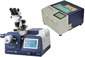
Sample Preparation
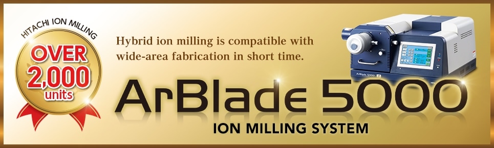
Ion milling system to prepare wide cross section of a sample, ion sputter to increase the conductivity of non-conductive sample and sample cleaner to reduce contamination which disturb electron microscope observation.
*1 Scanning Electron Microscope
*2 Transmission Electron Microscope
*3 Scanning Transmission Electron Microscope
*4 Focused Ion Beam systems
Related topics
“S.I.navi” is Hitachi Membership Site for analytical instruments users.
“S.I.navi” provides helpful information for daily analysis.

Hitachi High-Tech Social Media