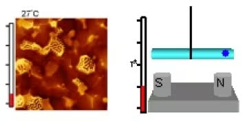
Physical property evaluation conducted using Environmental Control Unit AFM
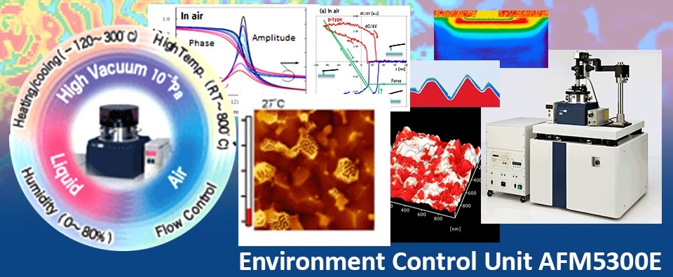
To determine the impact of various environmental conditions on measurement data, AFM physical property observation was performed using the AFM5300E environmentally controlled atomic force microscope under several different environments, including open-air, dry nitrogen, high vacuum, liquid submersion, and heating/cooling/humidity-controlled.
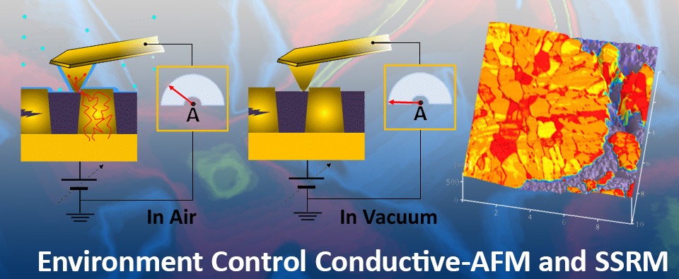
1. Conductive-AFM, SSRM for measurement of electric current and resistance in open-air/vacuum environments
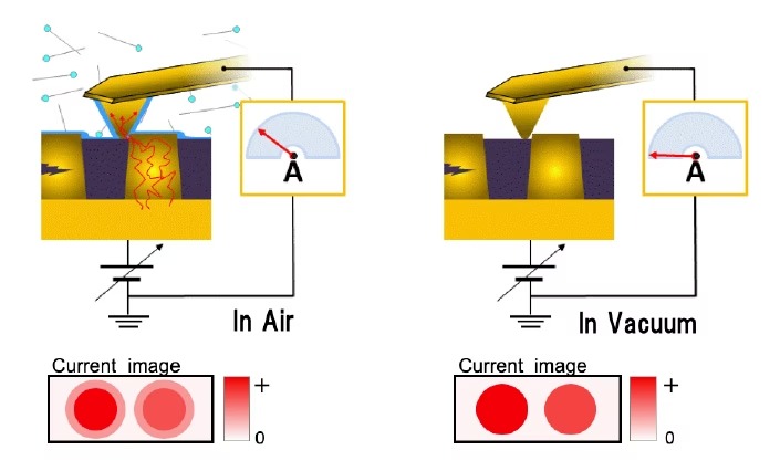
(1) The effects of adsorbed water on Conductive AFM observation of SRAM
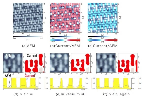
Figure 1-1(a) shows the polished surface topography of SRAM (Static Random Access Memory) manufactured with a 22 nm process. The characteristic pattern seen in the topography is the SRAM’s metallic conduit wiring. Just below that is the PMOS or NMOS, which is connected to gates and other transistor elements. Figure 1-1(b, c) shows an image of current distribution taken with Conductive-AFM (C-AFM) and overlapped with an AFM image. The electric current stemming from the BIAS voltage inversion (±1 V) is shown as positive current in red and negative current in blue. This shows us the conductive properties that respond to the structure below the conduit wiring.
Figure 1-1(d-f) shows the C-AFM observation results for a portion of the SRAM in open-air and vacuum environments, followed by open-air again, in that order. It displays the AFM image and the cross-sectional profile of the current. We can see that the red region where electric current passes is more enlarged in open-air environments than vacuum. From this, we can surmise that during observation in open-air environments, the adsorbed water covering the surface of the sample and tip had an impact.
(2) Verifying the effects of adsorbed water on the force-current curve
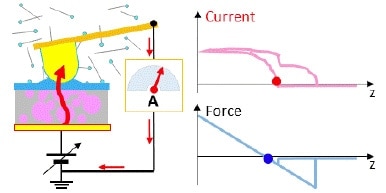
In Figure 1-2, the normal out-bound/in-bound force curve measurement is coupled with electric current (force-current curve). This enables the simultaneous evaluation of local mechanical energy and electric conduction properties. Through this, we can see that the in-bound and out-bound current curves are not consistent, since electric current flows while the tip is being pulled by the adsorbed water. When the tip is isolated from adsorption and made completely non-contact, electric current is also reduced to zero.

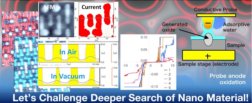
(3) Measurement of the HOPG force-current curve in open-air/vacuum environments
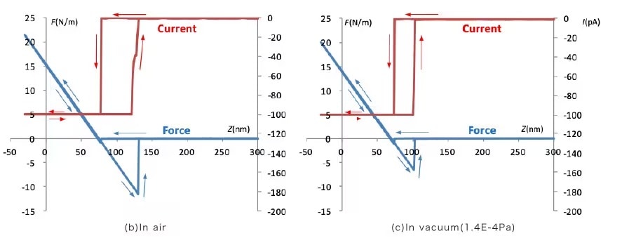
Image 1-3 shows the force current curve of HOPG (Highly Orientated Pyrolitic Graphite) in open-air/vacuum environments. HOPG has hydrophobicity, but when viewing in open-air and vacuum environments, we see a difference in both the force curve and the current curve. Adsorption is greater in the open-air environment and occurs over greater distances between the tip and sample. In the current curve, we see a difference in conductivity only in the precise sections where adsorption occurs in the tip and sample.
(4) The impact of adsorbed water on C-AFM and SSRM measurements
By evaluating the force-current curve in Figure 1-3, we see that electrical current is traveling through the adsorbed water. We can surmise that the current is traveling through the adsorbed water even while the tip makes contact with the sample during scanning and an actual example of this can be seen in Figure 1-1, which shows the results of C-AFM observation of SRAM.
In Figure 1-4, we see current and a video model of the observed current distribution in the time during scanning. Even when the tip separates from the edge of the conductive parts, current continues to flow through the adsorbed water in open-air environments and that portion alone accounts for the expansion seen in the current. If the loss of current resolution due to adsorbed water is a concern, measurement in a high-vacuum environment will prove effective. *
* The high resolution of SSRM when observing the concentrated distribution of semiconductor carriers in high-vacuum environments has already been acknowledged in the 2011 and 2013 editions of the international semiconductor technology roadmap.
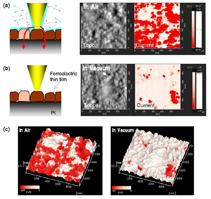
(5) C-AFM measurement of ferroelectric film in open-air/vacuum environments
Figure 1-5(a, b) shows the C-AFM measurement results for ferroelectric film on Pt, as well as the analogous model video which shows electrical conduction between the tip and sample. In the C-AFM observed current distribution imaging of the electrodes on the sample side with -7 V of superimposed voltage applied, negative current is shown running in the red portion. Compared to the open-air environment, there are far fewer regions with current running in the vacuum environment. In the vacuum environment, a portion of the ferroelectric crystals and grain boundaries where leakage occurred have current running through them, but in the open-air environment, we can surmise that the current traveled through adsorbed water on the surface to a wider region. If the objective of observation is to identify the areas with leakage, this suggests that such information will be hidden by the adsorbed water. Since Figure 1-5(c) shows the correlation between topography, structure and physical properties, it consists of 3-D topography with overlapping current contrast. This enables understanding with a single glance of which crystals, grain boundaries, and other areas are conducting current.
(6) The effects of anodizing on C-AFM and IV measurements
Previously, we showed how surface water adsorption is reflected in current or force-current graphs, but here we will introduce cases where surface adsorption of water actually changes the surface topography. In Figure 1-6, we see the results when +2 V of current is applied to Si wafer samples while the tip proceeds in open-air and high-vacuum environments, after which the voltage was reduced to 0 V and a broad stretch of the surrounding region was observed for its topography. Observation reveals a topography swelling of 1 nm in areas that were scanned after 2 V was applied in the open-air environment, while in the high-vacuum environment, we see little to no change.
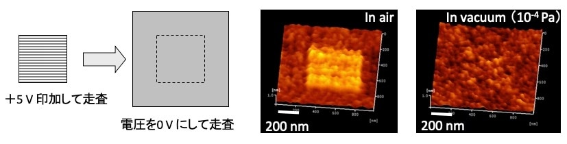
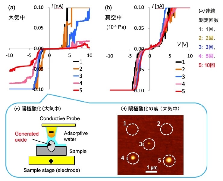
Figure 1-7 (a, b) shows the results when any of 5 points on the Si wafer are continuously measured for I-V in open-air and high-vacuum environments. The number of continuous I-V measurements will be set as 1, 2, 3, 5, and 10 times, while each area that is measured will be given a number 1-5. In addition, the I-V curve is represented in the average of the continued measurements. When measuring in the vacuum environment, a stable I-V curve was obtained, regardless of the number of measurements, but when measuring in the open-air environment, electrical current decreased as the number of measurements increased.
Figure 1-7 (d) shows the surface topography after I-V continuous measurement of 5 locations in the open-air environment. The areas where continuous I-V measurement occurred show swelling, while the height of and diameter of protrusion grow with each episode of I-V measurement. In Figure 1-6 as well, this phenomenon reflects how, during open-air measurement only, topography swelling occurs in the areas where electrical current has been applied.
The reason that swelling was seen in the Si wafer’s topography in those areas where electrical current was applied is anodization. Figure 1-7 (C) shows the anodization mechanism. When electrical current is applied between the tip and sample, the ion OH- within the adsorbed water in the surrounding area causes anodization. In the open-air environment, the reason that electrical current decreases as the number of continuous I-V measurement episodes increases is a result of growth in the thickness of this anodization.
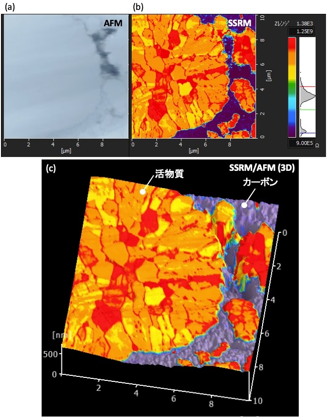
(7) SSRM observation in a high-vacuum environment of lithium-ion batteries with positive electrodes
When lithium-ion battery fuel is exposed to an open-air environment, the effects of moisture and oxygen in the atmosphere cause a scientific reaction and alteration to the surface, making observation in a high-vacuum environment preferable. Figure 1-8 shows the results of SSRM observation of a sample of lithium-ion battery cathodes. In the SSRM image, we see the errors in electrical resistance within each crystal in the cathode active material, the fact that the grain boundaries are more resistant than the crystals, and the fact that electrical resistance occurs in the conducting agent surrounding the active material at an order of magnitude smaller than the active material itself.
2. SNDM measurement of dopant distribution in open-air/dry nitrogen/vacuum environments
(1) SNDM to detect changes in capacitance
In the previous section, we verified the (open-air/high-vacuum) environmentally sourced error that occurs when using C-AFM or SSRM to detect direct current. We learned the impact on the detection of current, I-V curve, and other electrical properties that is caused when current travels the adsorbed water on the surface and the anodizing that occurs beneath the water.
Adsorbed water is formed by H2O molecules and its dielectric constant is 80 polar molecules, a number that is larger than the dielectric constant of Si and SiO2 (approx. 12 and 3.8 respectively). Now, we shall compare the capacitance of surfaces covered with water molecules in an open-air environment to that of surfaces in a high vacuum.
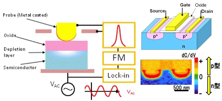
Here, we verify the impact of adsorbed water when SNDM (scanning nonlinear dielectric microscope) is used to detect capacitance after applying AC voltage between the tip and sample.
Figure 2-1 shows observed results of changes in capacitance detected with SNDM and a schematic diagram of an Si MOS FET cross section and dopant distribution.
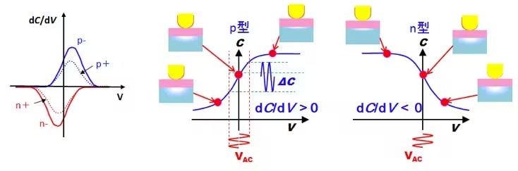
With SNDM, AC voltage is applied between the tip and sample while an FM demodulator is used to detect the changes in dC/dV capacitance below the tip as frequency changes on the approximately 1 GHz quasi-microwave hunting oscillation circuit. When AC current of this type is applied to a MOS structure consisting of tip (metal M), oxidation zone (O), and semi-conductor (S), the depletion layer modulates as seen in the animation and MOS capacitance shifts. With p and n-type semi-conductors, the behavior generated by modulation in the depletion layer is opposite, as seen in Figure 2-2. When the dC/dV signal is plus, it can be judged as p and when it is minus, it can be judged as n. In known actual cases of detection performed on Si MOS FET cross sections, as well, the p diffusion layer can be easily seen in the n region.
* For a detailed explanation regarding SNDM, visit the “Explanation of AFM working principle” page.
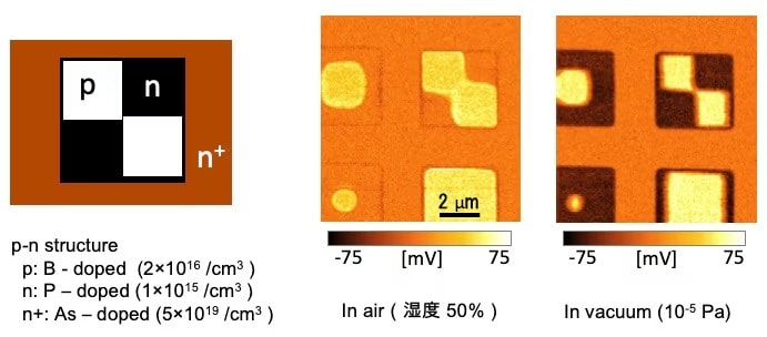
(2) SNDM observation of a sample with p-n doping pattern under humidity-controlled or high-vacuum environments
Figure 2-3 displays the results of SNDM observation of a sample with p-n doping pattern, in both a controlled environment with 50% humidity and a high vacuum. We can see that the P region is bright (dC/dV > 0), while the n region is dark (dC/dV < 0). Compared to the high-vacuum environment, the p region in the 50% humidity state is swelled.*
* Ando, Kazunori; Kuramochi, Hiromi; Hasumura, Satoshi; Watanabe, Kazutoshi; Yokoyama, Hiroshi. “Capacitance measurement nonlinear dielectric microscopy”, Hyomen Kagagu Vol. 25. No. 5, pp. 296―299 (2004)
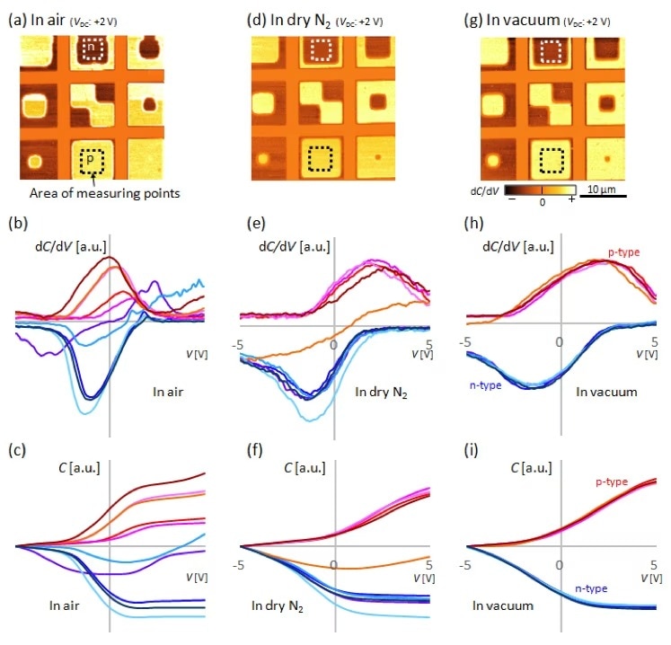
(3) dC/dV-V, C-V characteristics in open-air, dry nitrogen and high-vacuum environments
Figure 2-4 shows cumulative data for the SNDM observation results, as well as the dC/dV-V and C-V curve of a sample with p-n doping pattern in open-air (approx. 30% humidity), dry nitrogen (99.995% pure N2 gas) and high-vacuum (10-4 Pa) environments. In each environment, while the measurement point within the broken line was gradually shifted, voltage was swept away on the sample side and a measurement of the dC/DV-V curve was performed 10 times, alternating 5 times each between the p side and n side. In addition, the dC/dV-V curve was integrated to calculate the C-V curve (However, the integrated figures were not yet determined at the point in time shown in the figure).
When comparing the SNDM images from each environment, a small n-type spot on the lower right of the image can be seen in the dry nitrogen and high-vacuum environments. In the open-air environment, however, this spot is hidden by pH signals and cannot be observed.
When observing the dC/dV-V curve in an open-air environment, differences emerge in the curve with each measurement and even when measuring the n region, the curve reflects the fact that the p-side signal has been received. In the dry nitrogen environment, the variation between the dC/dV-V and C-V curves is less than in the open-air environment. In the high-vacuum environment, the variation between the dc/dV-V and C-V curves is much less, and the curve obtained is close to the theoretical dC/dV-V and C-V characteristics (Figure 2-2).
Other than the modulation of the depletion layer that occurs in response to dopant density, the impact at the sample surface level of the doped oxidation layer, stored charge and undulations is well known. From the results of this experiment, however, we can see that measurement atmosphere, especially the existence of adsorbed water on the surface, also has an impact. *
※ Jing-jiang Yu, T. Yamaoka, S. Hasumura, R. Hirose, K. Ando, and K. Mizuguchi: "Environmental control scanning nonlinear dielectric microscopy measurements of p-n structures, epi-Si Wafers, and SiC crystal defects", ISTFA 2015: Conference Proceedings, 341-348, 2015.
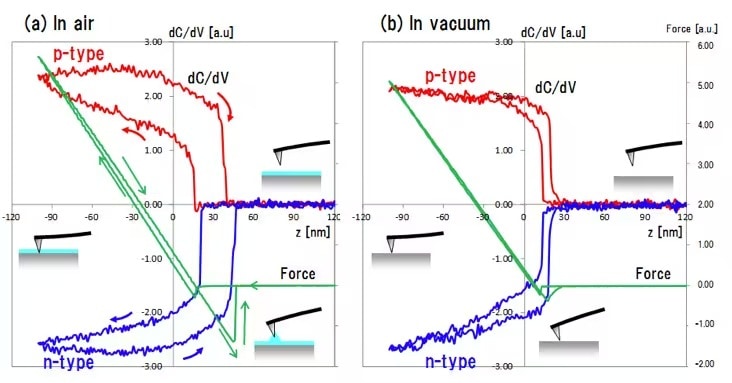
(4) The force-dC/dV curve that occurs in open-air and high-vacuum environments
In the previous section, we explained about force-current curves, but here we will examine dC/dV type force-dC/DV curves (see Figure 2-5). In an open-air environment, the dC/dV value never reaches 0 while the tip makes contact, as it is covered in adsorbed water. The behavior generated by adsorption when the tip makes contact and then separates at the in-bound and out-bound ends of the force curve impacts the dC/dV measurement and generates large variation in dC/dV at the in and out points. In vacuum environments, there is still a slight variation due to tip adsorption, but it can be said to be much smaller than the impact in open-air environments. We can thus conclude that SNDM and dC/dV measurements performed in open-air environments include variation caused by adsorbed water.*
* Takehiro Yamaoka: “Melding SNDM and PM electromagnetic property observation with SEM observation”, Japan Institute of Microscopy, Scanning Probe Microscope Subcommittee, Proceedings, pp. 25-30, Makuhari Messe, September 7, 2016.
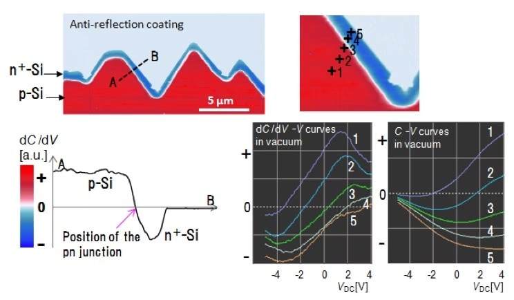
(5) Actual examples of dC/dV-V and C-B curve measurements in high-vacuum environments (Si solar cells, SiC power MOS transistors)
Figure 2-6 shows an actual case of SNDM measurement and dC/dV-V, as well as C-V curve measurement in the pn junction for Si solar cells. Color bar options are reflected as red for p-type and blue for n-type. The white color in-between displays shows the pn junction in the SNDM image and cross-sectional signal profile. In addition, the traditional C-V characteristics are also detected in the pn junction seen in the 5-point dC/dV-V and C-V curves, during those cases when the p region crosses the pn junction to the n region.
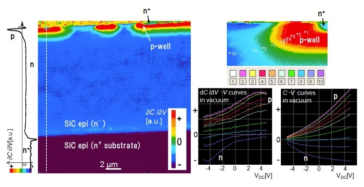
Figure 2-7 is an actual case showing SNDM and dC/dV-V measurements for SiC power MOS transistors in a vacuum environment. From the SNDM image, we can see the distribution of dopant density in response to the device’s structure. The 10-point dC/dV-V and V-V curves that cross the pn junction from the p region to the n region both indicate that traditional C-V characteristics were detected. *
* AFM application data sheet No.8: “Observation via SNDM of dopant distribution in a cross section of a SiC power device,” Hitachi High-Tech
3. MFM for observation of electric resistance - magnetic domain in open-air/vacuum environments
(1) MFM observation of magnetic recording media and cantilever vibrations in open-air and vacuum environments
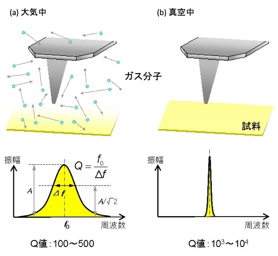
MFM (Magnetic Force Microscopes) and EFM (Electron Force Microscopes) detect electromagnetic interaction between the tip and sample as shifts in cantilever resonance. Here, we can verify the differences between the physical property measurements that cause the cantilever to vibrate in open-air and vacuum environments.
Figure 3-1 shows a model of the cantilever vibrations in open-air and vacuum environments. In an open-air environment, air molecules collide constantly with the tip and the sample surface, impacting the state of the cantilever vibrations. On the other hand, in a vacuum environment, there are few to no gas molecules and there is no impact on the state of the cantilever vibrations. This can be seen with a single glance at the cantilever vibration spectrum (Q-curve). The sharpness of the vibration spectrum index is reflected as a Q value. Q values are a dimensionless quantity calculated by dividing the resonant frequency by the width of the resonance curve. In open-air environments, the vibration spectrum broadens due to the collision of air molecules and the Q value reaches approximately 100 to 500. On the other hand, since there are few to no gas molecules in a vacuum environment, the value will reach several thousands. Since the sensitivity of electromagnetic measurements is similar to q values, vacuum environments are advantageous for such highly sensitive scanning. In addition, since the cantilever vibrations are not impacted by viscosity resistance in vacuum environments, it is possible to achieve more stable electromagnetic measurement.
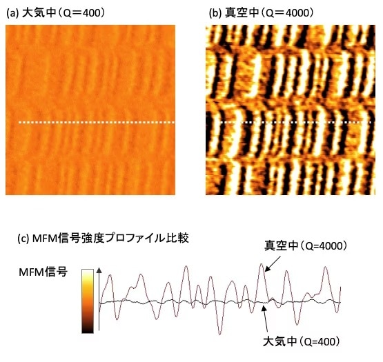
Figure 3-2 (a, b) shows the results of MFM measurement of identical portions of magnetic recording media in open-air and vacuum environments. To aid comparison, MFM contrast options are set at identical levels. Figure 3-2 (c) shows the broken line signal strength profile of each MFM image. In comparing the open-air environment to the vacuum environment, Q level gain is near equal, while sensitivity is improved ten-fold.
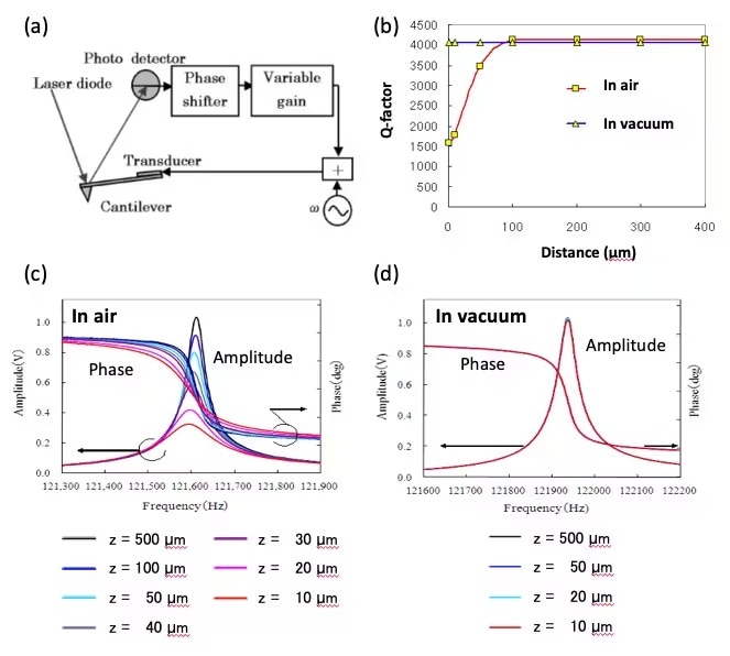
(2) Regarding the Q value control technology that enables highly sensitive electromagnetic measurement in vacuum environments
Highly sensitive electromagnetic measurements performed in vacuum environments, like those seen in Figure 3-2, are made possible by the Q value control techniques seen in Figure 3-3(a). Q value control techniques are a method in which the cantilever vibration phase is shifted π/2 and amplified, allowing increase or decrease of Q value via electronic circuits that recycle the cantilever vibrations. The sensitivity of electromagnetic measurements is analogous to Q value, meaning that the higher the Q, the greater the sensitivity. On the other hand, response works in inverse proportion to Q value, so when Q exceeds 10000 in a vacuum environment, measurements will grow unstable. The MFM image in Figure 3-2(b) shows the results of MFM measurement when Q value is held to 4000 via Q value control techniques.
Figure 3-3 (b-d) shows the results when the distance dependence of the amplitude curve and phase curve are measured in open-air and vacuum environments with Q value limited to 3000 on a tip 500 μm in height and brought within 10 μm of the sample. When the tip is brought close in the open-air environment, an increase in viscosity resistance causes a shift to resonant frequency with low vibration voltage and a reduction in amplitude, leading to a broad resonance peak. Due to this, the Q value also decreases as the tip gets closer. In addition, the slope of the phase curve also gets smaller. In a vacuum environment, even when the tip gets close, the resonance curve and phrase curve change very little, illustrating superior stability. *
*
Yamaoka, Takehiro; Watanabe, Kazutoshi; Shirakawabe, Kiharu; Chinone, Kazuo: “Development of a highly sensitive, high-resolution MFM system”, Journal of the Magnetics Society of Japan, 27, pp. 429-433 (2003).
T. Yamaoka, K. Watanabe, Y. Shirakawabe, K. Chinone, E. Saitoh, M. Tanaka, and H. Miyajima: IEEE Trans. Magn., 41, pp. 3733-3735 (2005).
(3) Application in cases of nano-magnetic observations using Q value control in vacuum environments
Since MFM are used to detect the magnetic force that operates on magnetic tips and magnetic samples, it is possible to increase MFM sensitivity by applying a magnetic film coating to the magnetic tip, giving it greater thickness. However, this will reduce resolution and as we see in Figure 3-4(a), the tip’s stray magnetic field disrupts the magnetic state of the soft magnetic material and nano-magnetic sample, leading to a deformed magnetic domain structure. Combined use of MFM in a Q controlled vacuum environment and a low-moment MFM probe with a thin magnetic coating enables high-resolution observation without disrupting the magnetic domain structure.
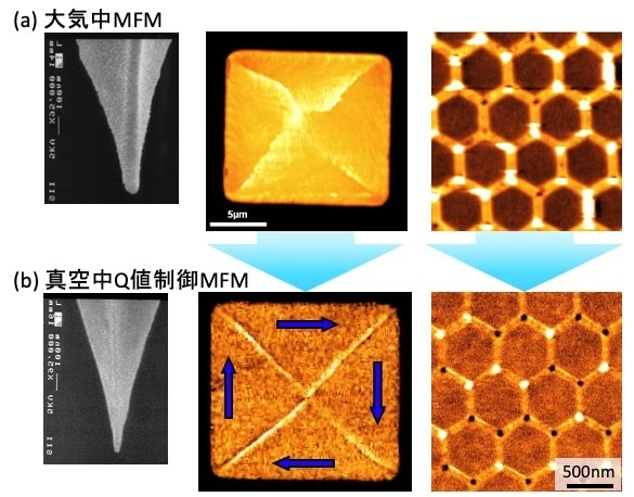
Here, we will introduce other reports about applications for MFM when performing nano-magnetic observation in a Q controlled vacuum environment.
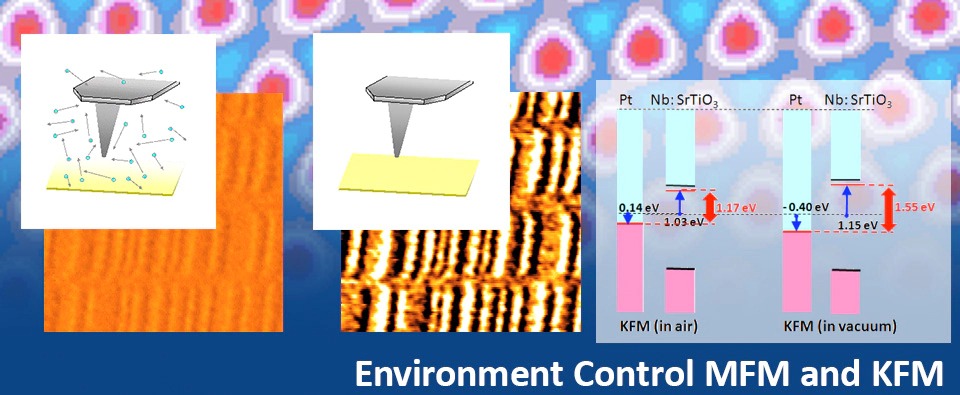
4. KFM for evaluation of electric resistance - work functions in open-air/vacuum environments
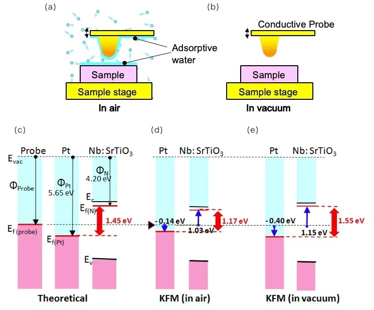
KFM (Kelvin Probe Force Microscopy) is used to measure the difference in contact potential (surface potential) that is equivalent to the difference in work functions between the conductive tip and sample. *
Figure 4-1 is a model image of KFM measurement data in vacuum open-air and vacuum environments, displaying the results of KFM measurement on a Pt and Nb doped section of a SrTiO3 sample as a banded electronic energy structure. The difference in fermi level obtained from the literature data for Pt and Nb doped SrTiO3 is expressed in Figure 4-1(c) as 1.45 eV, while KFM resulted in results of 1.17 eV in the open-air environment, as expressed in Figure 4-1(d), and 1.55 eV in the vacuum environment, as expressed in Figure 4-1(e). The vacuum environment has obtained measurements closer to the values in the literature data. From this, we can surmise that atmospheric components such as the adsorbed water on the sample surface and tip, or humidity, have an impact on surface potential calculations.
* Evaluating work functions in open-air and vacuum environments with a single atomic force microscope (AFM Application Data Sheet No. 7)
5. Heated or chilled measurement in vacuums
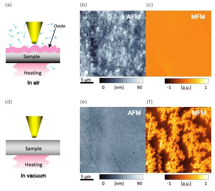
(1) Actual case of heated measurement of a neodymium magnet with MFM in open-air and vacuum environments
Figure 5-1 is a surface topography and magnetism image for measurements performed on a neodymium magnet while heating to 150°C in open-air and vacuum environments. When heating in the open-air environment, harsh thermal oxidation causes rough undulations on the surface to grow bigger. In addition, since thermal oxidation results in loss of magnetism, no magnetic signal is displayed in the MFM image.
When heating in a vacuum environment, there is no impact from oxidation and a flat surface topography image has been obtained that is no different from surface topography at room temperature, and a clear magnetic domain structure is observed. *
* T. Yamaoka et al, " Vacuum magnetic force microscopy at high temperatures: Observation of permanent magnets" , Microscopy Today, 22, 6, 12-16, 2014.
The advantage of heated measurement in a vacuum environment is that the heating does not generate impact from atmospheric gases. In addition, the surface of the cantilever that faces the sample surface is also heated by gas molecules, meaning that there is less warping of the cantilever in vacuum environments as well. When the AFM measurement environment is changed to a dry inactive gas environment, such a step will prove somewhat effective in dealing with the impact of water adsorption and oxidation, but it cannot prevent the convection that results from heating.
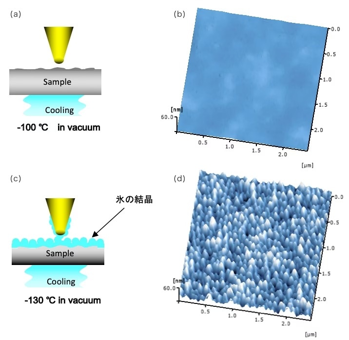
(2) Chilled measurement in vacuum environments (countermeasures against ice and crystal formation)
When temperature is reduced below dew point in open-air environments, water adheres to surfaces. Typically, coagulation begins near 0°C. For this reason, chilled measurements are performed in a vacuum environment.
Figure 5-2 shows surface topography when a sample section of a semiconductor has been cooled in a vacuum environment near 10-5 Pa. At -100°C, a result nearly identical with topography at room temperature was obtained, but when cooling reached -130°C, crystals began to form.
Even if the measurement environment is changed to a dried, highly pure inactive gas environment, the residual amount of water molecules and impure gases will still be of a greater magnitude than in the vacuum environment and as such, it is not realistic to perform measurement at temperatures as low as -100°C under atmospheric pressure conditions. Thus, high-vacuum environments are highly effective, even in cases of sample cooling.
(3) Other actual cases of AFM physical property observation during heating and cooling
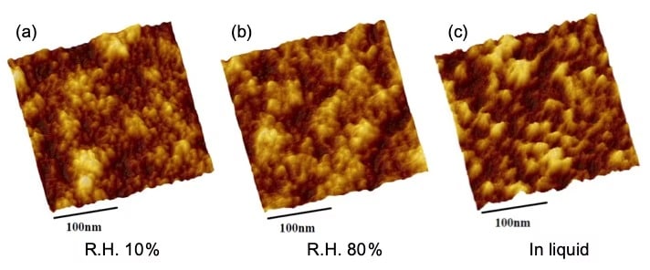
6. AFM observation of electrolyte membrane fuel cells in low-humidity/high-humidity/liquid environments
In addition to the previously mentioned open-air, high-vacuum, heated and chilled environments, the environmentally controlled atomic force microscope AFM5300E also includes options applicable to measurement during inert gas replacement, moisture control and liquid submersion. Figure 6-1 illustrates the capabilities of these environmental control options by showing the results of AFM observation of electrolyte membrane fuel cells in low-moisture (10%), high-moisture (80%), and pure water environments. When moisture is high, you can see how the electrolyte membranes absorb water and swell to a larger size. In pure water, this swelling is even more pronounced, and we see a shift to rough surfaces.*
* Application to fuel cells: Observation of electrolyte membranes in moisture controlled and pure water environments (AFM Application Brief No. 59)
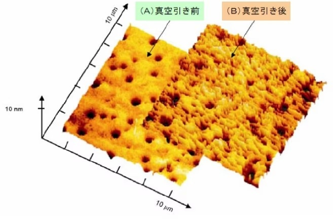
8. Actual cases where vacuum observation was not suitable
In some polymer materials, volatile components such as low-molecular-weight components and residual solvents are sublimated or vaporized from the surface, leading to changes in material surface structure or composition. Figure 8-1 shows structural changes observed with AFM in film-shaped polymer materials before and after approx. 30 minutes of evacuation. After evacuation, we see the emergence of surface roughness with undulations multiple nm in height.*
* Observation of structural changes occurring within film-shaped polymer materials in a vacuum environment (AFM Application Brief No. 41)
Product lineup
Hitachi AFM will prove useful at any stage
By application
Automation / Ease of use
High accuracy / High resolution
- High-accuracy measurements of slanted surfaces with a steep slope
- High-accuracy measurements without damaging samples
- High-resolution measurements in a vacuum
- Stable and accurate measurements during sample heating and cooling
- High-accuracy topography measurements
- High-sensitivity MFM measurements in ambient or vacuum environments
- Humidity control / observations in liquid
Physical property measurements /
Environmental Controls
- Measurements of work functions in ambient or vacuum environments
- Observations of dopant distribution
- Quantitative measurements of elastic modulus
- Observations of structural changes in a vacuum
- Enabled true observations of topography and other physical properties
- Enabled quantitative measurements during sample heating and cooling
This section introduces applications (actual measurement cases) for scanning probe microscopes (SPM/AFM).
Information for product users
This section offers information aimed at customers who use our scanning probe microscopes.
For first-time users
Related topics

“S.I.navi” is Hitachi Membership Site for analytical instruments users.
“S.I.navi” provides helpful information for daily analysis.


Hitachi High-Tech Social Media