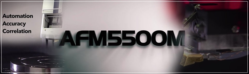
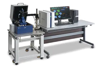
Scanning Probe Microscopes (SPM/AFM)

Hitachi AFM will prove useful at any stage
View by applications
Automation / Ease of use
High accuracy / High resolution
- High-accuracy measurements of slanted surfaces with a steep slope
- High-accuracy measurements without damaging samples
- High-resolution measurements in a vacuum
- Stable and accurate measurements during sample heating and cooling
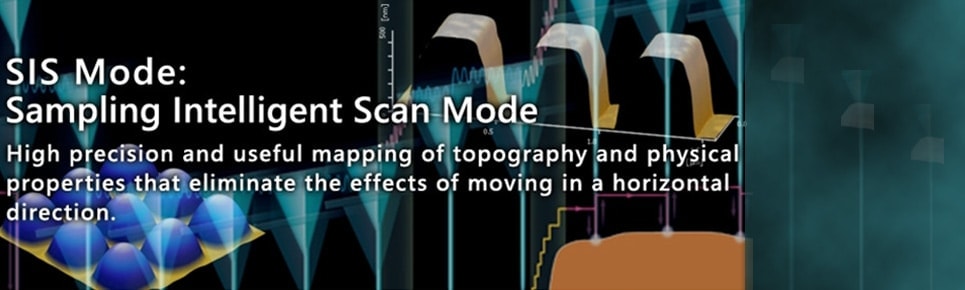
- High-accuracy topography measurements
- High-sensitivity MFM measurements in ambient or vacuum environments
- Humidity control / observations in liquid
Physical property measurements /
Environmental Controls
- Measurements of work functions in ambient or vacuum environments
- Observations of dopant distribution
- Quantitative measurements of elastic modulus
- Observations of structural changes in a vacuum
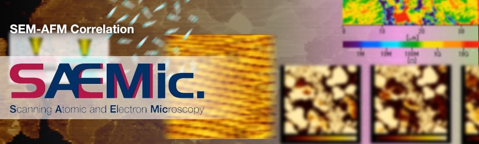
- Enabled true observations of topography and other physical properties
- Enabled quantitative measurements during sample heating and cooling
Product comparison
| Product name | ||
|---|---|---|
 |
 |
|
| Basic functions | (AFM100):AFM, DFM, PM, FFM, SIS-shapes (AFM100 Plus):AFM, DFM, PM, FFM, SIS-shapes/properties, Q-value control |
AFM, DFM, PM Phase, FFM |
| Function expandability* | SIS-ACCESS, LM-FFM, VE-AFM, Adhesion, MFM, EFM, KFM, PRM, Nano/Pico-Current, SSRM, Pico-STM*(AFM100 Plus only) | SIS topography, SIS material properties, LM-FFM, VE-AFM, Adhesion, Current, Pico-Current, SSRM, PRM, KFM, EFM(AC), EFM(DC), MFM |
| Applicable environments | Atmosphere, in liquid*, Heated*(*RT - 250°C), heated in liquid (RT -60°C) | Atmosphere |
| Fine positioning mechanism for samples | Manual stage XY: ±2.5 mm Impact stage (conductive type) |
Precise motor-driven stage Observable region: Entire 100 mm (4 inches) Stroke: Y ± 50 mm, Z ≥21 mm Minimum Step: XY 2 μm, Z 0.04 μm |
| Sample sizes | Maximum 35 mm diam., thickness 10 mm (max. 50 mm sq., thickness 20 mm)* |
Maximum 100 mm diam, thickness 20 mm |
*Optional
This section introduces applications (actual measurement cases) for scanning probe microscopes (SPM/AFM).
Information for product users
This section offers information aimed at customers who use our scanning probe microscopes.
For first-time users
Related topics

“S.I.navi” is Hitachi Membership Site for analytical instruments users.
“S.I.navi” provides helpful information for daily analysis.


Hitachi High-Tech Social Media