
Search by Industry - Logic
Logic
PRODUCT
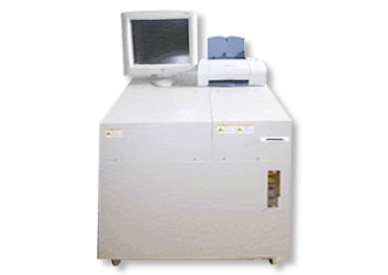
Process Gas Monitor
This system measures toxic components contained in gas in quite small quantity, small-quantity components adhered to material surfaces, etc., at high speed and high sensitivity.
PRODUCT
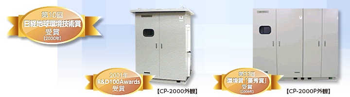
Dioxin Precursor /PCB Monitor CP-2000/CP-2000P
These monitors can measure and monitor the concentrations of chlorophenol and chlorobenzene contained in exhaust gas from garbage incinerator or the PCB concentration in PCB decomposing facilities continuously.
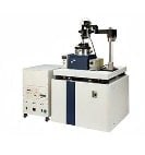
PRODUCT
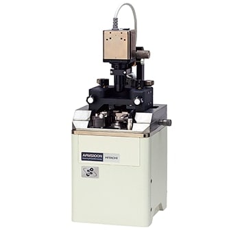
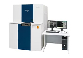
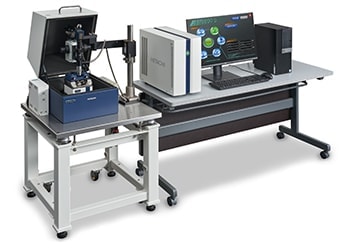
Probe Station AFM5000II / Real TuneII
Hitachi AFM5000II includes the control system and software package to allow a wealth of advanced imaging and data analysis. Its superb function RealTune enables the automatic and self-optimizing data acquisition for easier, faster, and more consistent collection of high-quality AFM images regardless of user skill level. It also provides a wide range of uncommon features such as Q control, tip calibration, and 3D overly for enhanced measurements and data processing.
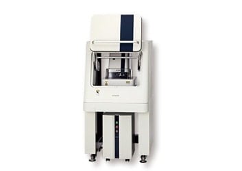
PRODUCT
General-purpose Small Unit AFM5100N
Hitachi's general-purpose atomic force microscope, Model AFM5100N, features superior ease of use, a wide range of capabilities, and extraordinary performance. The breakthrough hardware option, the self-sensing detector, doesn't require laser and detector alignments and thus can effectively simplify AFM operation. As a full-featured system in support of high-resolution and multifunctional AFM measurements, the AFM5100N offers a wide variety of advanced modes, including the proprietary sampling intelligent scan (SIS), which delivers previously unattainable results for very challenging samples.
PRODUCT
Environment Control Unit AFM5300E
The Hitachi research-grade AFM5300E offers significantly improved sensitivity, accuracy, and resolution of electromagnetic property measurements operated under high-vacuum conditions. Furthermore, it establishes a benchmark for comprehensive environmental control and is the only tool on the market affording AFM imaging in air/liquid/vacuum, a broad temperature range (-120 °C to 800 °C), magnetic field or humidity controls, as well as correlated AFM/SEM/ion milling investigations.
PRODUCT
Atomic Force Microscope AFM5500M
The AFM5500M is an AFM platform equipped with a fully addressable 4-inch stage, optimized for medium-sized samples. It affords exceptional levels of ease of use, automation, and accuracy, as well as correlation for AFM/SEM investigations.
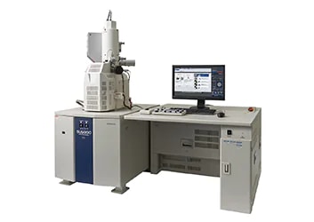
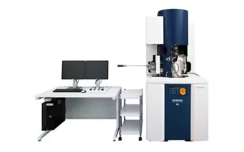
PRODUCT
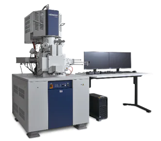
Schottky Field Emission Scanning Electron Microscope SU5000
Innovative analytical FE-SEM allows for a simple transition between high vacuum and variable pressure mode. EM Wizard is a knowledge-based system for SEM imaging that goes beyond basic preset conditions and recipes. Its ease of use opens a new gateway for material research, development, and area beyond our imagination.
PRODUCT
Ultra-High-Resolution Schottky Scanning Electron Microscope SU7000
SU7000: The Next-Generation FE-SEM The modern FE-SEM requires not only high performance but also a multitude of functionalities including wide-area observation, in-situ analysis, variable pressure, high-resolution imaging at low accelerating voltages, and simultaneous multi-signal collection. The SU7000 is designed to address these aspects and more by delivering enhanced information for diversified needs in the field of electron microscopy. Experience the nano-world with the SU7000!
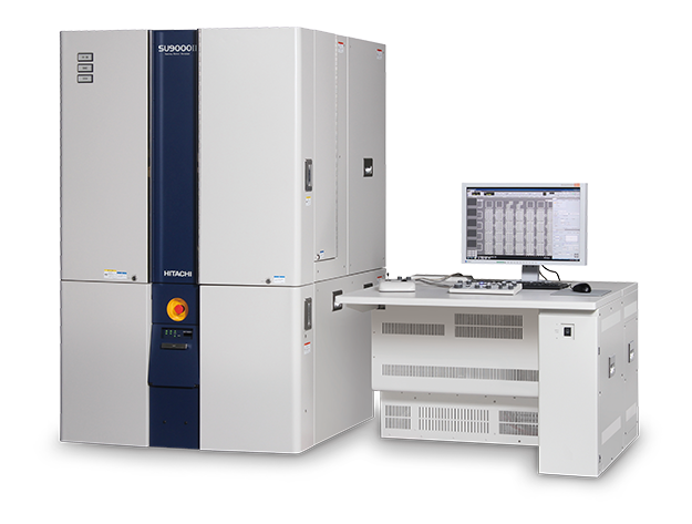
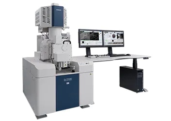
PRODUCT
Ultra-high Resolution Scanning Electron Microscope SU9000II
The Cold Field Emission source is ideal for high-resolution imaging with a small source size and energy spread. Innovative CFE Gun technology contributes the ultimate FE-SEM with superior beam brightness and stability, affording high-resolution imaging and high-quality elemental analysis.
To allow for stable data acquisition at the instrument‘s highest performance levels, the SU9000II offers new capabilities that render automated adjustments of the optical system—and the new EM Flow Creator software package as an option to render automated data acquisition, particularly sequential data collection.
In addition, unique optical system design has a capability of EELS for advanced material analysis.
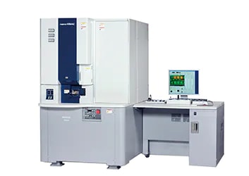
PRODUCT
Electron Beam Absorbed Current (EBAC) Characterization System nanoEBAC NE4000
The Hitachi NE4000 nanoEBAC is an electron beam based probing system for electrical characterization and EBAC analysis and imaging of microelectronic device interconnects, materials, and components.
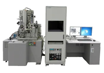
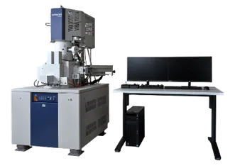
PRODUCT
Nanoscale Device Characteristics Analysis System Nano-Prober NP6800
The Hitachi NP6800 is a SEM-based dedicated probing system designed to meet the analytical needs of the 10-nm design node semiconductor device and beyond. The precision piezoelectric-driven actuator is equipped with X, Y and Z axes probe movements allowing the probes to be controlled very precisely for measuring the electrical characteristics of a single MOS transistor. The design concept was to create an easy-to-use probing system (like an optical probing system) while maintaining this same ease of operation even under the vacuum environment through our intuitive probe operation design.
PRODUCT
Scanning Electron Microscope FlexSEM 1000 II
The FlexSEM 1000 II VP-SEM combines innovative technological features with an intuitive interface, to deliver adaptability and flexibility in a powerful, automated, lab-friendly package. Cutting-edge technology and circuitry provides unrivaled imaging performance, even in variable-pressure environments, a feature previously only available in a full-sized SEM. This SEM runs on clean energy for an economical analytical tool, without compromising performance.
PRODUCT
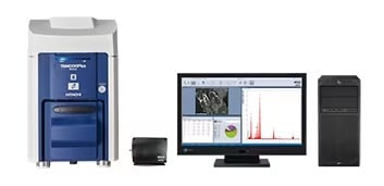
TM Series Energy Dispersive X-Ray Spectrometers: AZtec Series
The AZtec series offers multiple EDS systems to choose from based on application and budget. High-performance detectors with an energy resolution of 129 eV (Mn-Ka) are available in all classes.
PRODUCT
TM Series Energy Dispersive X-ray Spectrometer: Element series
Advanced EDS features for tabletop SEM Element series are EDX systems produced by EDAX Instruments. Si3N4 window SDD enhances the mapping speed and detection limits.
PRODUCT
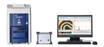
TM Series Energy Dispersive X-ray Spectrometer: Quantax75
The TM4000 Series offers multiple EDS systems to choose from based on application and budget. All detectors offered are of compact design and do not require LN2.
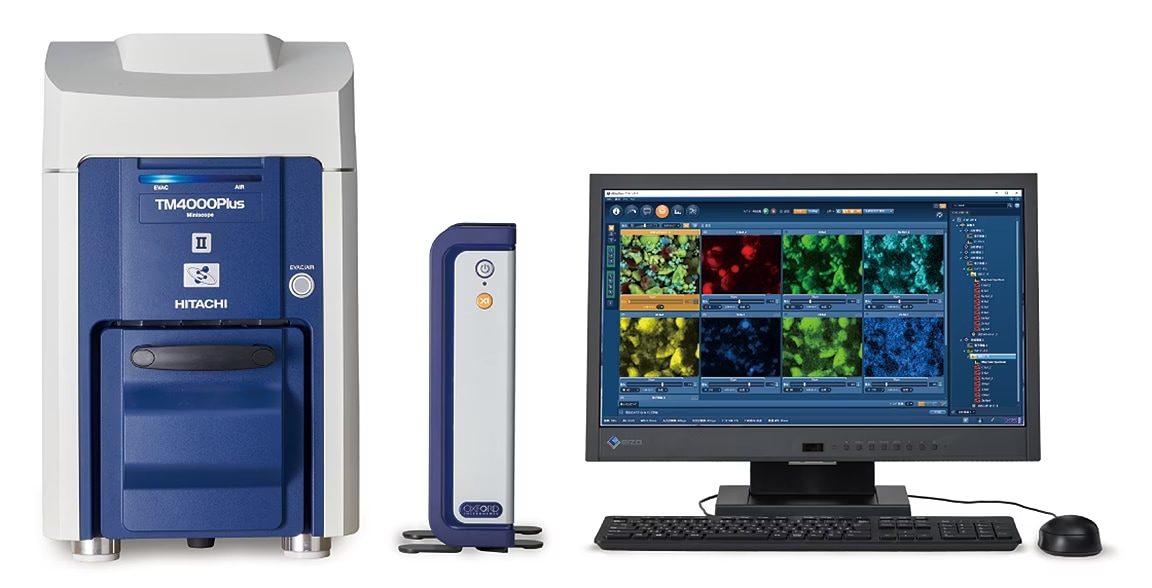
PRODUCT
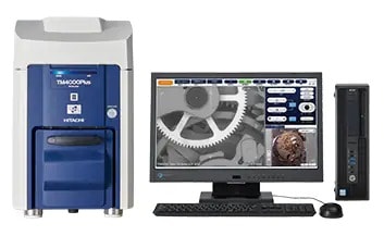
Tabletop Microscopes TM4000II / TM4000Plus II
The Future of Tabletop Microscopes is Here! The TM4000 Series features innovation and cutting-edge technologies which redefine the capabilities of a tabletop microscope. This new generation of the long-standing Hitachi tabletop microscopes (TM) integrates ease of use, optimized imaging, and high-image quality, while maintaining the compact design of the well-established Hitachi TM Series products. Experience the new dimension of tabletop microscopes with the Hitachi TM4000 II and TM4000Plus II.
PRODUCT
Field Emission Transmission Electron Microscope HF5000
Hitachi's unique 200 kV aberration-corrected TEM/STEM: the perfect harmony of imaging resolution and analytical performance 0.078 nm spatial resolution in STEM is achieved together with high specimen-tilt capability and large solid angle EDX detector(s), all in a single objective lens configuration. The HF5000 builds on features from Hitachi HD-2700 dedicated STEM including Hitachi's own fully automated aberration corrector, symmetrical dual SDD EDX and Cs-corrected SE imaging. It also incorporates the advanced TEM/STEM technologies developed in the HF series. Integrating these accumulated technologies into a new 200 kV TEM/STEM platform results in an instrument with an optimum combination of sub-Å imaging and analysis, as well as the flexibility and unique capabilities to address the most advanced studies.
PRODUCT
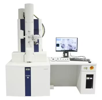
Transmission Electron Microscope HT7800 Series
The NEXT Generation of Innovation. Meeting and Exceeding Needs and Requirements in Many Fields. From biomedicine to nanomaterials The HT7800 RuliTEM is a 120 kV transmission electron microscope (TEM) with multiple lens configurations, including a standard lens for unsurpassed high contrast and a class-leading HR lens for high resolution. This breakthrough in advanced innovative design allows for highly efficient workflows and many specialized applications. It represents the cutting-edge solution for modern TEM analyses.
PRODUCT
Focused Ion Beam System MI4050
The MI4050 High-Performance Focused Ion Beam System is equipped with new optics and provides the world-leading SIM imaging resolution and high-definition TEM sample preparation with improved imaging resolution at low kV. The MI4050 accommodates a variety of applications such as cross-section observation, circuit modification, vector scan processing, nano-micro patterning, nano molding, and 3D nano fabrication using deposition function.
PRODUCT
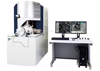
Focused Ion and Electron Beam System & Triple Beam System NX2000
Toward the ultimate TEM sample preparation system FIB-SEM systems have become an indispensable tool for characterization and analysis of the latest technologies and high performance nano-scale materials. An ever-increasing demand for ultrathin TEM lamellas without artifacts during FIB processing require the best in ion and electron optics technologies. Hitachi's NX2000 high performance FIB and high resolution SEM system with its unique sample orientation control* and triple beam* technologies, supports high throughput, and high quality TEM sample preparation for cutting edge applications.
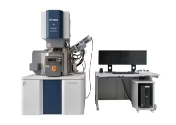
PRODUCT
Focused Ion and Electron Beam System Ethos NX5000 Series
Unsurpassed Performance with Ultimate Flexibility The Hitachi Ethos FIB-SEM incorporates the latest-generation FE-SEM with superb beam brightness and stability. Ethos delivers high-resolution imaging at low voltages combined with ion optics for nanoscale precision processing.
PRODUCT
Real-time 3D analytical FIB-SEM NX9000
FIB-SEM System for True 3D Structural Analysis The newly developed FIB-SEM system from Hitachi, the NX9000 incorporates an optimized layout for true high-resolution serial sectioning to tackle the latest demands in 3D structural analysis and for TEM and 3DAP analyses. The NX9000 FIB-SEM system allows the highest precision in material processing for a wide range of areas relating to advanced materials, electronic devices, biological tissues, and a multitude of other applications.
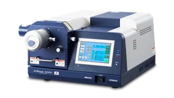
PRODUCT
Ion Milling System ArBlade 5000
The most advanced broad ion beam system for producing exceptionally high-quality cross-section or flat-milling samples for electron microscopy.
PRODUCT
Ultrahigh-Resolution Schottky Scanning Electron Microscope SU8700
The SU8700 brings in a new era of ultrahigh-resolution Schottky field emission scanning electron microscopes to the long-standing Hitachi EM lineup. This revolutionary FE-SEM platform incorporates multifaceted imaging, high probe current, automation, efficient workflows for users of all experience levels, and more.
PRODUCT
Ultrahigh-Resolution Scanning Electron Microscope SU8600
The SU8600 brings in a new era of ultrahigh-resolution cold-field emission scanning electron microscopes to the long-standing Hitachi EM lineup. This revolutionary CFE-SEM platform incorporates multifaceted imaging, automation, increased system stability, efficient workflows for users of all experience levels, and more.
PRODUCT
Multifunctional Probe Microscopy Platform AFM100 series
The AFM100 Series is Hitachi’s next generation probe microscopy platform. The AFM100 Plus and AFM100 systems that make up this series have been designed to expand the capabilities and performance of atomic force microscopy, while providing an easy-to-use platform suitable for users of all experience levels. Experience the finest reliability and innovation with the AFM100 Series.
PRODUCT
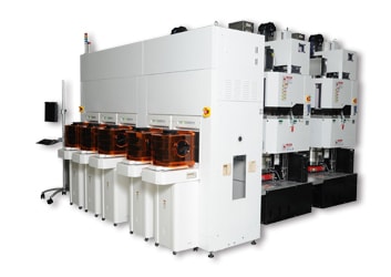
Conductor Etch System 9000 Series
Next generation devices at 20nm and below require double-patterning, 3D (three-dimensional) structures, and complex, high-precision processes that include protective layer formation and finishing techniques for new materials. Hitachi High-Tech developed the Conductor Etch System 9000 Series to support these next-generation processes.
PRODUCT
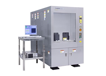
Advanced CD Measurement SEM CS4800
A sustainable CD measurement solution to a wide range of 4, 6, and 8 inch wafer Fabs The Advanced CD Measurement SEM CS4800 provides high-quality SEM imaging, improved measurement precision, and fast, automated operation, designed to improve productivity and operating efficiency of existing manufacturing lines and increase customer's process control capability. In addition, the CD-SEM: CS4800 can be configured to handle two different wafer sizes that can be switched by the customer using to a new wafer-transfer system. Hitachi High-Tech plans to expand support for various wafer materials such as Silicon Carbide (SiC) and Gallium Nitride (GaN) to meet diversified customer's needs for new semiconductor or electronic devices.
PRODUCT
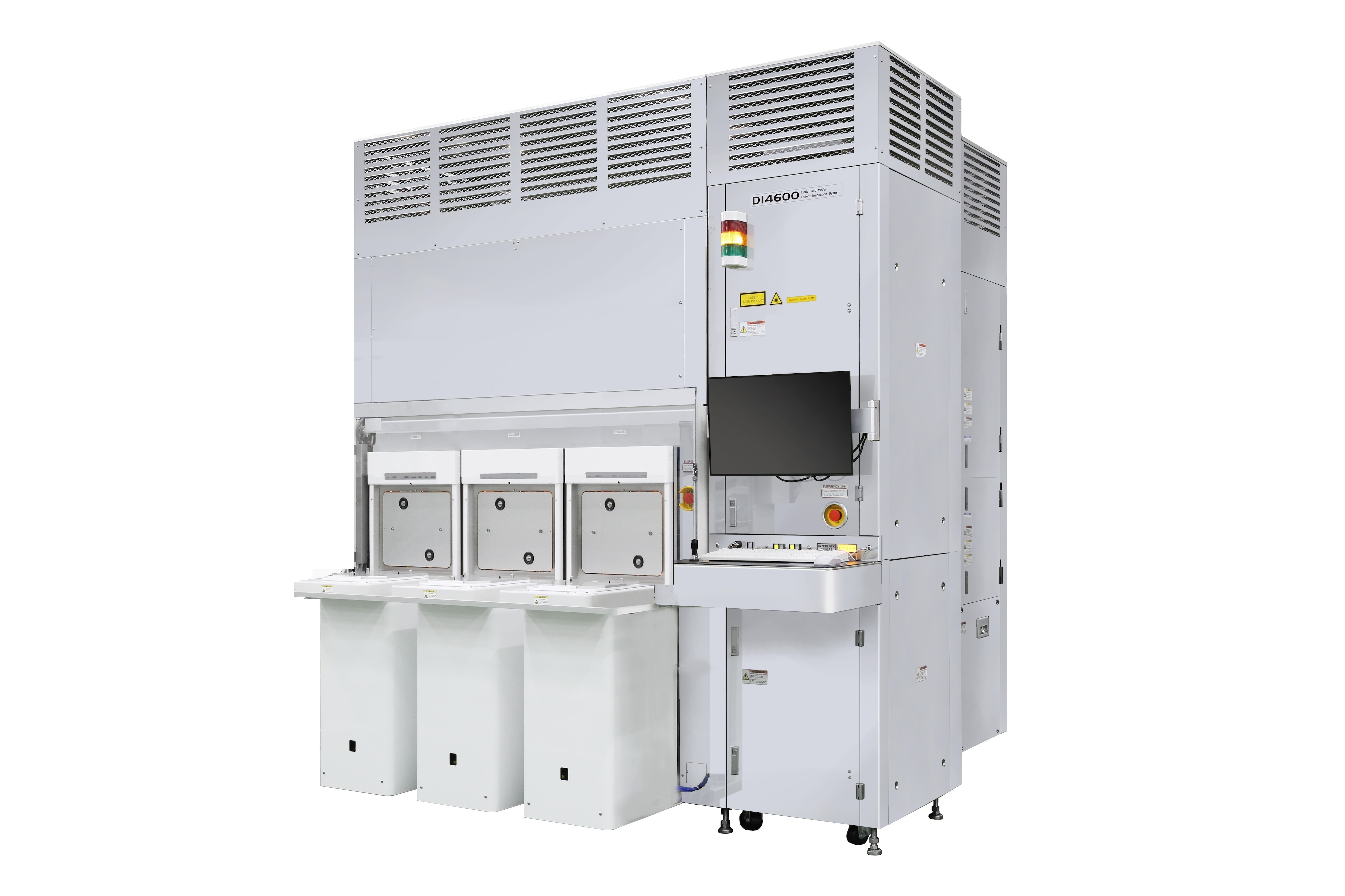
Dark Field Wafer Defect Inspection System DI4600
In the production lines of semiconductor fabs, abnormalities should be quickly detected to avoid yield loss.
To meet this need, DI4600 is designed to detect defects on patterned wafers with high sensitivity and throughput. High sensitivity and throughput are realized by the combination of the sheet-beam optics and the accurate light separation with spatial filters.
DI4600 systems are installed and running as in-line defect management tools in the cutting-edge memory and logic semiconductor fabs.
PRODUCT
Wafer Surface Inspection System LS Series
The wafer surface inspection system LS series can detect defects on unpatterned wafers with a mirror-finished surface. Applied technology of laser scattering achieves high sensitivity and high throughput detection of small contaminants and various types of defects on wafer surfaces prior to patterning. Wafer surface defects such as shallow scratch flatness defects, water marks, epi stacking faults, protrusions by the polishing process, and flatness defects caused during deposition cause problems in next-generation processes. The LS series achieve high sensitivity by detecting the light scattered from defects while suppressing background noise from the wafer surface. It is widely adopted to control contamination in the manufacturing of semiconductors on the 10-nm scale, and for delivery and incoming wafer quality control.
PRODUCT
Conductor Etch System M-8000 Series
Conductor Etch System M-8000 Series is utilized for hard mask and silicon etching for 32nm and beyond. Hitachi High-Tech developed new process flows, such as double patterning and new material etch processes such as high-k dielectric/metal gate through JDP (Joint Development Program) with device makers and material / tool suppliers. Hitachi High-Tech's etch system provides superior profile controllability and CD uniformity within wafer with a new microwave ECR (Electron Cyclotron Resonance) plasma etching chamber, high speed wafer temperature control, and high vacuum exhaust control technology. Hitachi High-Tech's AEC (Advanced Equipment Control) / APC (Advanced Process Control) technology with original data collection, analysis and control systems provide excellent productivity and reliability.
PRODUCT
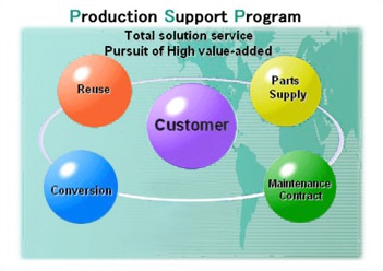
Production Support Program
Hitachi High-Tech provides the following production support programs with the concept of "achievement of total solution services to enhance the value-added equipment and to reduce operation cost."
PRODUCT
Advanced Area Inspection SEM GS1000
For the advanced device production – Large FOV area inspection SEM
PRODUCT
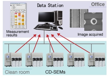
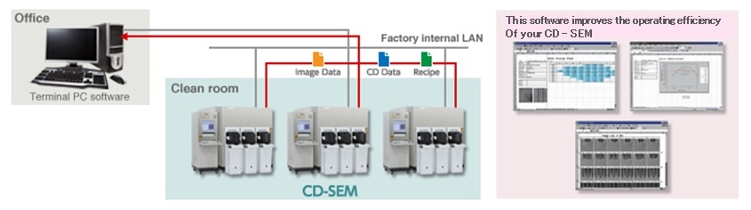
RecipeDirector / DesignGauge-AnalyzerPlus
RecipeDirector: Offline automated recipe creation without using a wafer by utilizing design data DesignGauge-AnalyzerPlus: Advanced data analysis station for CD-SEM images
PRODUCT
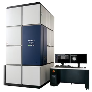
Advanced High Voltage CD-SEM “CV6300 Series”
CV6300 Series enables measurements of high aspect ratio deep holes and trench bottom dimensions to control the manufacturing of beyond 96 layers 3D NAND flash memory. CV6300 Series enables high speed and high precision overlay measurements for the advanced DRAM and Logic device.
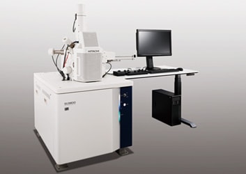
PRODUCT
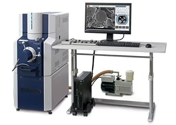
Scanning Electron Microscopes SU3800/SU3900
Performance & Power in a Flexible Platform Hitachi High-Tech's scanning electron microscopes SU3800/SU3900 deliver both operability and expandability. The operator can automate many operations and efficiently utilize their high performance. The SU3900 is equipped with a large multipurpose specimen chamber to accommodate observation of large samples.
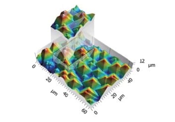
PRODUCT
3D Visualization Software Hitachi map 3D
Three-dimensional models allow Z-height Measurements Using Hitachi's latest high speed, 4-segment Backscattered Electron Detector, a three-dimensional model can be generated without sample tilting or manually collecting consecutive images.
PRODUCT
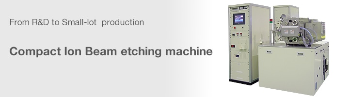
Micro-sampling System
This device is used for preparing the desired wafer part for analysis with STEM, TEM, etc. by extracting a micro sample with an ion beam in the vacuum chamber of an FIB system.
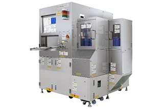
PRODUCT
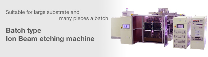
Batch type ion beam etching machine
Product information of Batch type ion beam etching machine.
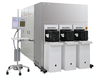
PRODUCT
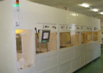
Batch Type Wet Station
Our system has batch type cleaning ,resist stripping and etching potions. All processes from chemical cleaning to dryer are fully automated.
PRODUCT
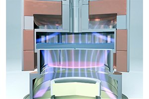
Microwave ECR Plasma Etch Chamber
Hitachi High-Tech's plasma chamber for conductor etch is based on an an ECR(Electron Cyclotron Resonance) plasma source, able to generate a stable high-density plasma at very low pressure (< 0.1 Pa). Microwave ECR plasma provides a wide process window in both R & D and mass production through accurate plasma parameter management, such as plasma distribution or plasma position control. The same plasma control technology is also applied to dry cleaning to maintain a more stable chamber condition.
PRODUCT
Defect and Pattern Evaluation SEM CT1000
3D observation capability contributing “to Shorten development cycle“ and “to enhance product quality“ of G&C device*1 Once a wafer of up to 200 mm in size has been transported automatically, CT1000 moves precisely to the critical pattern position, or the defect position detected by the defect inspection unit. Three-dimensional SEM observation can then be performed using a tilting sample stage. CT1000 also has an energy-dispersive X-ray spectrometer (EDS) *2 that can be used to infer the elements contained in the sample for observation.
PRODUCT
Dark Field Wafer Defect Inspection System DI2800
Contribution to defect detection and high-level process control of G&C device*1 DI2800 uses scattering-intensity simulation technology to optimize the illumination and detection optics, enabling highly sensitive inspection of patterned-wafer defects developed during the manufacturing process. It has a detection sensitivity of 0.1-μm standard particle size on mirrored wafers. This makes it possible to examine even the incredibly small, 0.3-mm square size chips used in semiconductor devices in the IoT and automotive fields, with optimization of the inspection sequence enabling a defect inspection speed of over forty 200-mm wafer sheets per hour.
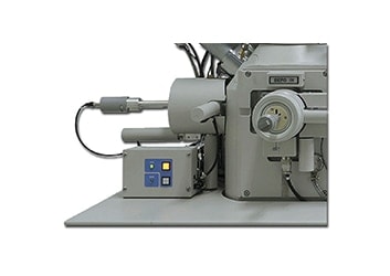
PRODUCT
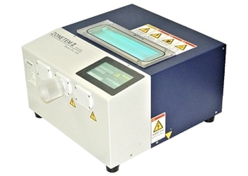
Sample Cleaner ZONETEM II
The innovative ZONETEM II Desktop Sample Cleaner uses UV-based cleaning technology to minimize or eliminate hydrocarbon contamination for electron microscopy imaging. ZONE offers easy-to-use cleaning for pre-analysis sample preparation, ensuring the best possible data from your TEM samples.
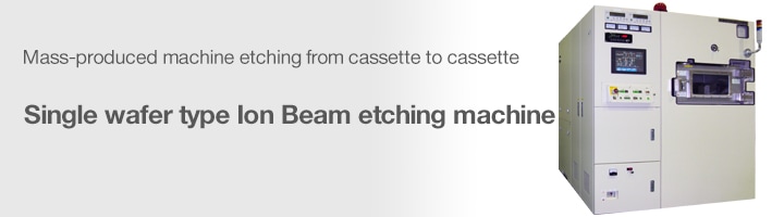
PRODUCT
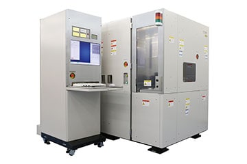
Single wafer type ion beam etching machine
Product information of Single wafer type ion beam etching machine.