![]()
AKAFUJI (Mt. Fuji in Red)
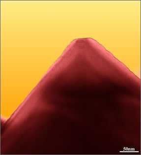
© Takuji Miyamoto (Instrument Division, Hitachi, Ltd.)
The AKAFUJI, or "Mt. Fuji in Red", is actually crystallized tungsten oxide (2/10,000 mm in size) photographed with a transmission electron microscope. The crystal was formed and developed by heating tungsten in a very low oxygen pressure. A series of steps can be observed along the slope with each step measuring about 2/10 millionths of a millimeter representing the layer of atoms. The study of crystal formation is a significant work which is one of the basic technologies for semiconductor industry but also for material sciences.
Prize winning photo at 52nd photo contest hosted by the Japanese Society of Electron Microscopy in 1996.
Condition
Instrument : Transmission Electron Microscope H-9000NAR
Magnification : × 300,000
Accelerating voltage : 300 kV
Processing Condition
Heating temperature : 1,200°C
Gas pressure : 1.0 × 10⁵ Pa
*All information related to these photographers is based on the information when the photo was taken.
*This work was presented at the "photo contest" hosted by the Japanese Society of Microscopy.
*Reproduction or republication without permission prohibited.
*"nanoart" is registered trademark of Hitachi High-Tech Corporation in Japan.
Products & Services
Related Information

Hitachi High-Tech Social Media