Nano Stained glass
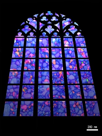
This image shows the result of TKD (Transmission Kikuchi Diffraction) crystal orientation analysis of the Cu electric wiring, in which fine grains of the crystal are the pseudo-colored as the color crystal map. This technique using transmission electrons enables us to see the orientation map of the tens nm grain which could not be visualized by the conventional method with backscattered electrons. The grain orientation map is like the stained glass made of the fine crystals.
At 70th photo contest hosted by the Japanese Society of Microscopy in 2014.
Condition
Specimen : Cu electric wiring
Instrument: Focused Ion & Electron Beam System nanoDUE'T NB5000
Magnification : X 50,000
Accelerating voltage : 30 kV
*This work was presented at the "photo contest" hosted by the Japanese Society
of Microscopy.
*Reproduction or republication without permission prohibited.
*"nanoart" is registered trademark of Hitachi High-Tech Corporation in Japan.
Products & Services
Related Information

Hitachi High-Tech Social Media