![]()
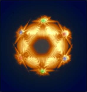
Star Crest
© Hisafumi Ohtsuka (Hitachi High-Tech corporation)
This is a Large Angle Convergent Beam Electron Diffraction (LACBED) pattern observed along Si (111) zone axis. Convergent electron beam produces such beautiful geometrical patterns formed by perfect atomic arrangement. Could you call it a "CREST of material"?
At 58th photo contest hosted by the Japanese Society of Electron Microscopy in 2002.
Condition
Specimen: Si single crystal
Instrument: Transmission Electron Microscope H-9000NAR
Accelerating voltage: 200 kV
*All information related to these photographers is based on the information when the photo was taken.
*This work was presented at the "photo contest" hosted by the Japanese Society of Microscopy.
*Reproduction or republication without permission prohibited.
*"nanoart" is registered trademark of Hitachi High-Tech Corporation in Japan.
Products & Services
Related Information

Hitachi High-Tech Social Media